

 Call Us Now !
Tel : +86 755 27374946
Call Us Now !
Tel : +86 755 27374946
 Order Online Now !
Email : info@bichengpcb.com
Order Online Now !
Email : info@bichengpcb.com
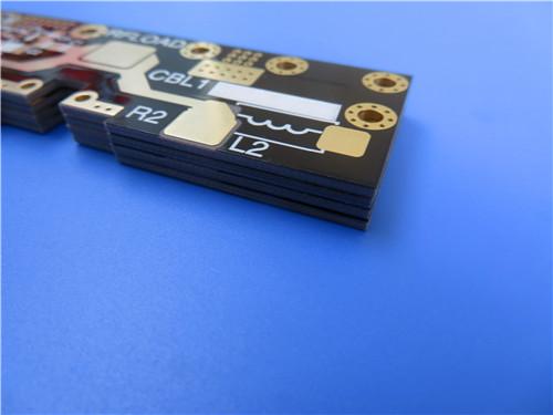
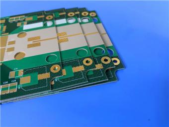
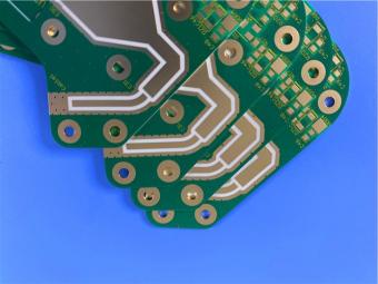
The F4BTME350 2-layer ENIG PCB combines high-frequency electrical performance, mechanical stability, and manufacturing quality.
Item NO.:
BIC-628-v713Order(MOQ):
1-10Payment:
T/TProduct Origin:
ChinaShipping Port:
ShenzhenLead Time:
7-10 days
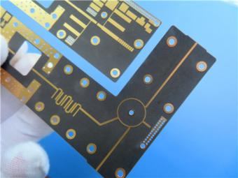
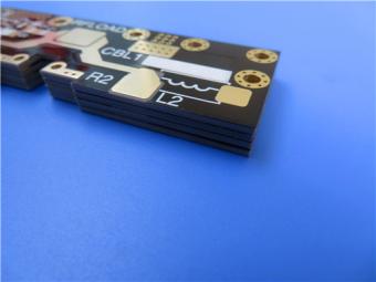
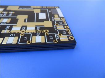
Wangling F4BTME350 10mil DK3.5 High Frequency Substrate PCB 2-Layer Immersion Gold
High-Frequency Product Description & CCL Material Reference
The F4BTME350 2-layer immersion gold PCB is a high-frequency board built on a PTFE-based ceramic-filled laminate, offering Dk 3.5 ±0.07 at 10 GHz and Df 0.0025. At 0.3 mm finished thickness with 1 oz copper and immersion gold finish, it targets 4G/5G antennas, LNAs, phased arrays, satellite communications, and automotive radar where signal integrity and PIM performance are critical.
This DK3.5 F4B PCB is a precision 2-layer rigid board for RF and microwave applications. Its substrate combines PTFE resin, glass fiber cloth, and nano-ceramic fillers to achieve a controlled Dk of 3.5 with ultra-low loss. The 0.3 mm finished thickness suits compact high-density modules. Every unit is 100% electrically tested and manufactured to IPC-Class-2 standards.
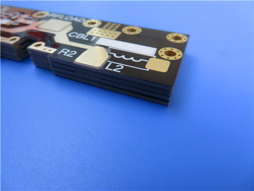
The table below summarizes the complete construction specifications.
|
Parameter |
Specification |
|
Base Material |
F4BTME350 |
|
Layer Count |
2 layers (rigid) |
|
Board Dimensions |
89.77 × 45.16 mm, ±0.15 mm |
|
Min Trace / Space |
6 / 8 mils |
|
Min Hole Size |
0.25 mm |
|
Blind Vias |
None |
|
Finished Thickness |
0.3 mm |
|
Finished Cu Weight |
1 oz (35 µm) outer layers |
|
Via Plating |
20 µm |
|
Surface Finish |
Immersion gold |
|
Top Silkscreen |
White |
|
Bottom Silkscreen |
None |
|
Top Solder Mask |
Black |
|
Bottom Solder Mask |
None |
|
Electrical Test |
100% prior to shipment |
|
Quality Standard |
IPC-Class-2 |
|
Artwork Format |
Gerber RS-274-X |
|
Availability |
Worldwide |
3. PCB Stackup
The symmetric 2-layer stackup uses copper outer layers and a single F4BTME350 core.
|
Layer |
Material |
Thickness |
|
Cu Layer 1 (Top) |
Copper |
35 µm (1 oz) |
|
Core |
F4BTME350 |
0.254 mm (10 mil) |
|
Cu Layer 2 (Bottom) |
Copper |
35 µm (1 oz) |
The component and interconnect counts reflect a focused RF design.
|
Metric |
Count |
|
Components |
12 |
|
Total Pads |
38 |
|
Thru-Hole Pads |
17 |
|
Top SMT Pads |
21 |
|
Bottom SMT Pads |
0 |
|
Vias |
9 |
|
Nets |
2 |
· Dk 3.5 ±0.07 at 10 GHz enables tight 50-ohm impedance control.
· Df 0.0025 at 10 GHz / 0.0035 at 20 GHz minimizes insertion loss.
· CTE 10/12 ppm/°C (x/y), 51 ppm/°C (z) from -55 to 288°C ensures stability.
· PIM ≤ -160 dBc via reverse-treated RTF copper foil.
· Moisture absorption ≤0.05%; thermal conductivity 0.54 W/(m·K).
· UL-94 V-0; operating temperature -55 to +260°C.
· 4G/5G base station antennas
· LNAs, LNBs/LNCs
· Phased array and phase-sensitive antennas
· Satellite communications, aerospace equipment
· Microwave/RF modules, radar (incl. automotive)
· High-power amplifiers, passive components
· PCS/PCN large-format antennas, feed networks
The F4BTME350 ENIG PCB combines high-frequency electrical performance, mechanical stability, and manufacturing quality. Its PTFE ceramic-filled substrate, tight Dk tolerance, ultra-low loss, and PIM below -160 dBc suit demanding RF designs. Backed by IPC-Class-2 certification, 100% electrical testing, and worldwide availability, it offers a reliable platform for next-generation communication systems.
Part II: F4BTME350 CCL Material Knowledge
The F4BTME350 copper clad laminate is part of the F4BTM/F4BTME series by Taizhou Wangling Insulation Materials Factory. It is formulated from glass fiber cloth, nano-ceramic fillers, and PTFE resin under strict pressing. Built on the F4BM dielectric layer, nano-ceramics enhance Dk, heat resistance, insulation, and thermal conductivity while preserving low loss.
Both share the same dielectric but use different copper foil. F4BTM pairs with ED copper foil for non-PIM applications. F4BTME pairs with reverse-treated RTF foil, delivering PIM ≤ -160 dBc, precise line control, and lower conductor loss — ideal for high-performance antenna and phase-sensitive systems.
· Dk selectable 2.98–3.5 (F4BTME350 = 3.5)
· Nano-ceramic enhanced performance
· Excellent PIM (F4BTME: ≤ -160 dBc)
· Thickness 0.254–12.0 mm; multiple panel sizes
· High-volume, cost-effective production
· Radiation-resistant, low outgassing
The table below presents the full datasheet for Wangling F4BTME350.
|
Property |
Test Condition |
Unit |
Value |
|
Dk (typical) |
10 GHz |
— |
3.5 |
|
Dk Tolerance |
— |
— |
±0.07 |
|
Df (typical) |
10 GHz |
— |
0.0025 |
|
Df (typical) |
20 GHz |
— |
0.0035 |
|
Dk Temp Coefficient |
-55 to 150°C |
ppm/°C |
-60 |
|
Peel Strength (F4BTM) |
1 oz |
N/mm |
>1.6 |
|
Peel Strength (F4BTME) |
1 oz |
N/mm |
>1.4 |
|
Volume Resistivity |
Normal |
MΩ·cm |
≥10⁷ |
|
Surface Resistance |
Normal |
MΩ |
≥10⁶ |
|
Elec. Strength (Z) |
5 kW, 500 V/s |
kV/mm |
>32 |
|
Breakdown Voltage (XY) |
5 kW, 500 V/s |
kV |
>40 |
|
CTE (XY) |
-55 to 288°C |
ppm/°C |
10, 12 |
|
CTE (Z) |
-55 to 288°C |
ppm/°C |
51 |
|
Thermal Stress |
260°C, 10 s, 3x |
— |
No delamination |
|
Moisture Absorption |
20±2°C, 24 h |
% |
≤0.05 |
|
Density |
Room temp |
g/cm³ |
2.20 |
|
Long-Term Use Temp |
Thermal chamber |
°C |
-55 to +260 |
|
Thermal Conductivity (Z) |
— |
W/(m·K) |
0.54 |
|
PIM (F4BTME only) |
— |
dBc |
≤-160 |
|
Flammability |
— |
UL-94 |
V-0 |
|
Composition |
— |
— |
PTFE + glass fiber; ED or RTF foil |
Test methods: Dk via GB/T 12636-1990 or IPC-TM-650 2.5.5.5 (Z-direction stripline); other properties per IPC-TM-650 or GB/T 4722-2017. Data are typical values.
|
Series |
Foil Type |
Thicknesses |
|
F4BTM |
ED |
0.5, 1, 1.5, 2 oz |
|
F4BTME |
Reverse RTF |
0.5, 1 oz |
|
Size (mm) |
Note |
|
460 × 610 |
Standard |
|
600 × 500 |
Standard |
|
914 × 1220 |
Not for thickness ≥ 4.0 mm |
|
Thickness (mm) |
Tol. (mm) |
Thickness (mm) |
Tol. (mm) |
|
0.254 (min) |
±0.02 |
1.524 |
±0.06 |
|
0.508 |
±0.04 |
2.0 |
±0.075 |
|
0.762 |
±0.05 |
3.0 |
±0.09 |
|
0.8 |
±0.05 |
4.0 |
±0.1 |
|
1.0 |
±0.05 |
5.0 |
±0.1 |
|
1.016 |
±0.05 |
6.0 |
±0.12 |
|
1.27 |
±0.06 |
8.0 |
±0.15 |
|
|
|
10.0 |
±0.18 |
|
|
|
12.0 |
±0.2 |
Copper- or aluminum-backed versions offer enhanced shielding and heat dissipation. Naming: F4BTM(E)-AL or -CU.
|
Model |
Base |
Density |
Thermal Cond. |
Base Thickness (mm) |
|
-CU |
Copper |
8.9 g/cm³ |
380 W/mK |
0.48–3.98 |
|
-AL |
Aluminum |
2.7 g/cm³ |
180 W/mK |
0.48–3.98 |
Base tolerance: +0.02/-0.05 mm. Sizes: 460×610, 460×305 mm.
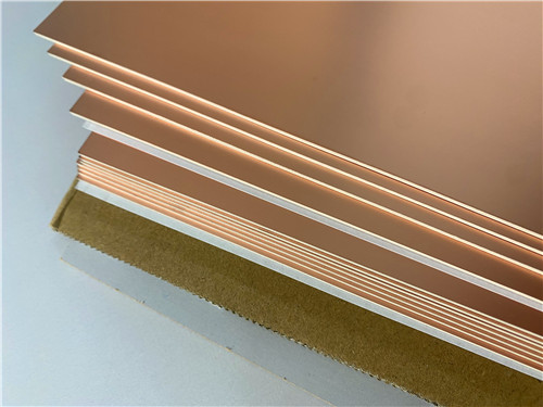
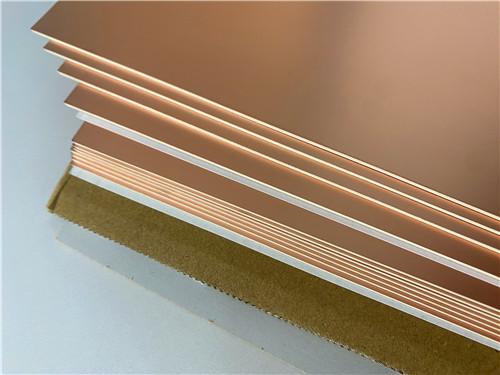
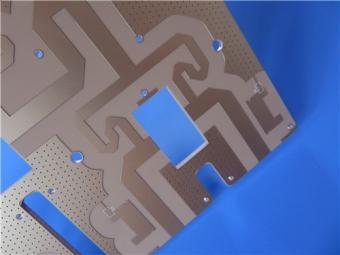
Figure 1: F4BTME350 PTFE-based copper clad laminate
The F4BTME350 substrate is a versatile PTFE-based laminate that underpins the PCB in Part I. Its nano-ceramic composition, reverse RTF foil, broad thickness and size options, and metal-backed variants give RF designers a flexible, reliable substrate. All properties are validated via IPC-TM-650 and GB/T methods, providing data confidence for high-frequency design across 4G/5G, satellite, aerospace, and automotive radar applications.
Previous:
Wangling F4BTMS220 2-Layer DK2.2 PCB 10 mil Core with Immersion GoldNext:
Wangling F4BTM300 Custom 2-layer PCB 20mil DK3.0 Substrate with Immersion GoldIf you have questions or suggestions,please leave us a message,we will reply you as soon as we can!
Categories
New Products
Wangling F4BTMS220 2-Layer DK2.2 PCB 10 mil Core with Immersion Gold
Wangling F4BTME350 10mil DK3.5 High Frequency Substrate PCB 2-Layer Immersion Gold
Wangling F4BTM300 Custom 2-layer PCB 20mil DK3.0 Substrate with Immersion Gold
Rogers 20mil RT/duroid 6202 2-layer ENIG High-Frequency Microwave PCB
Rogers 20mil AD250C PCB Pure Gold High-Frequency Antenna Circuit Board
8-Layer Hybrid RF PCB: RO4350B + TG170 FR-4 + RO4003C with RO4450F Bondply
4-Layer Rogers RO3010 Hybrid PCB Immersion Silver 2.8mm Finished Thickness
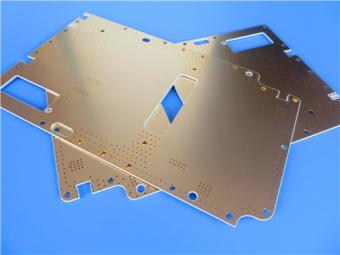
4-Layer 20mil Rogers RO3210 ISIG High-Frequency PCB with Controlled Depth Milling
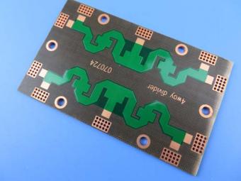
Polytetrafluoroethylene (Short for PTFE), commonly known as "plastic king ", is a polymer compound made of tetrafluoroethylene by polymerization. It has excellent chemical stability, corrosion resistance, sealing, high lubrication and non-viscosity, electrical insulation and good aging resistance.
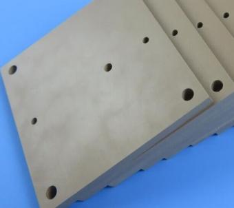
Rogers TMM4 thermoset microwave material is ceramic, hydrocarbon, thermoset polymer composite designed for high plated-through-hole reliability stripline and microstrip applications.
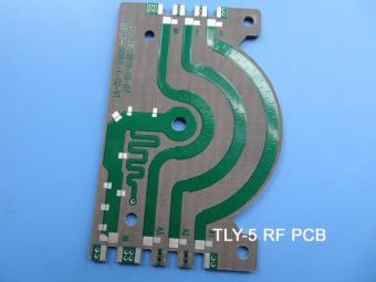
Taconic TLY laminates are a type of low loss laminates. They are manufactured with very light weight woven fiberglass and are more dimensionally stable than chopped fiber reinforced PTFE composites.
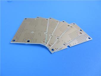
RO3203 laminates combine the surface smoothness of a non-woven PTFE laminate, for finer line etching tolerances, with the rigidity of a woven-glass PTFE laminate. These materials can be fabricated into printed circuit boards using
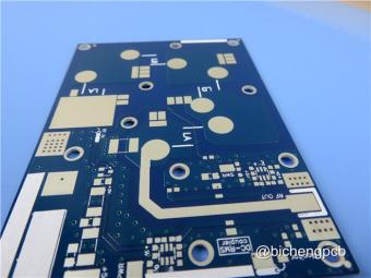
This type of immersion silver RF PCB is made on one of Taconic’s ORCER family material: RF-45.
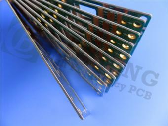
Rogers’ TMM10 thermoset microwave materials are ceramic, hydrocarbon, thermoset polymer composites designed for high plated-thru-hole reliability stripline and microstrip applications.
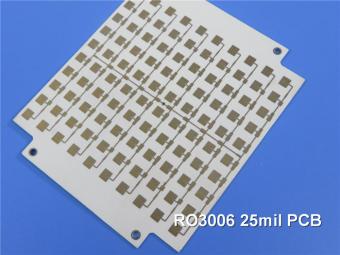
Rogers RO3006 was designed to offer exceptional electrical and mechanical stability at competitive prices.
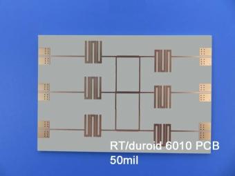
RT/duroid 6010LM microwave laminates feature ease of fabrication and stability in use. This property results in the possibility of mass production and reducing the cost of goods.
 6-11C Shidai Jingyuan, Fuyong, Baoan, Shenzhen, Guangdong, China 518103


For inquiries about our products or pricelist, please leave to us and we will be in touch within 24 hours.
© Copyright: 2026 Shenzhen Bicheng Electronics Technology Co., Ltd.. All Rights Reserved.

IPv6 network supported


