

 Call Us Now !
Tel : +86 755 27374946
Call Us Now !
Tel : +86 755 27374946
 Order Online Now !
Email : info@bichengpcb.com
Order Online Now !
Email : info@bichengpcb.com
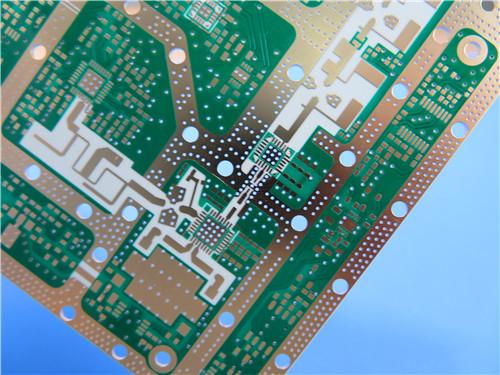
This article presents a Rogers RO4360G2 2-layer PCB on a 12 mil (0.305 mm) core with ENEPIG finish, built for small-cell transceivers and base-station power amplifiers.
Item NO.:
BIC-630-v715Order(MOQ):
1-10Payment:
T/TProduct Origin:
ChinaShipping Port:
ShenzhenLead Time:
7-10 days
RO4360G2 Rogers 12mil ENEPIG 2-Layer DK6.15 High Frequency Custom PCB
This article presents a Rogers RO4360G2 2-layer PCB on a 12 mil (0.305 mm) core with ENEPIG finish, built for small-cell transceivers and base-station power amplifiers. Its construction, stackup and design statistics are summarized below in three tables, followed by an in-depth look at the RO4360G2 laminate itself, including its full data sheet and material photograph.
1. The RO4360G2 12 mil ENEPIG PCB
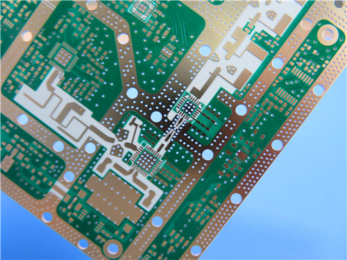
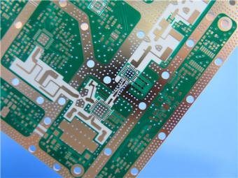
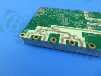
The board is a double-sided, single-core RF panel measuring 48.9 × 95.4 mm. Rogers RO4360G2 is clad with 1 oz electrodeposited copper on both faces; plated-through holes carry 20 μm copper, giving a finished thickness of 0.4 mm. ENEPIG on the top side yields a flat, bondable nickel-palladium-gold surface for fine-pitch SMT, while the absence of blind vias keeps processing conventional. Green solder mask and white silkscreen appear on the top only; the bare bottom preserves the microstrip reference plane. Artwork is Gerber RS-274-X, the board meets IPC-Class-2, and every unit is 100% electrically tested.
The board’s key mechanical and finishing attributes are listed in Table 1.
|
Parameter |
Value |
|
Base material |
Rogers RO4360G2 |
|
Layer count |
2 layers |
|
Board dimensions |
48.9 mm × 95.4 mm (1 piece) |
|
Minimum trace / space |
5 / 7 mils |
|
Minimum drilled hole |
0.4 mm |
|
Blind / buried vias |
None |
|
Finished board thickness |
0.4 mm |
|
Finished copper weight |
1 oz (1.4 mils), outer layers |
|
Via plating thickness |
20 μm |
|
Surface finish |
ENEPIG (top side) |
|
Top silkscreen |
White |
|
Bottom silkscreen |
None |
|
Top solder mask |
Green |
|
Bottom solder mask |
None |
|
Artwork format |
Gerber RS-274-X |
|
Acceptance standard |
IPC-Class-2 |
|
Electrical test |
100% prior to shipment |
Table 1. PCB construction details.
The two-layer stackup places equal copper on both faces of a single 12 mil core (Table 2).
|
Layer |
Material / Description |
Thickness |
|
Layer 1 (top) |
Electrodeposited copper |
35 μm |
|
Core |
Rogers RO4360G2 substrate |
12 mil (0.305 mm) |
|
Layer 2 (bottom) |
Electrodeposited copper |
35 μm |
Table 2. PCB stackup (2-layer rigid).
The design is modest in component count but dense in RF routing, as shown in Table 3.
|
Item |
Count |
|
Components |
20 |
|
Total pads |
34 |
|
Thru-hole pads |
18 |
|
Top SMT pads |
16 |
|
Bottom SMT pads |
0 |
|
Vias |
21 |
|
Nets |
2 |
Table 3. PCB design statistics.
Three choices merit note. ENEPIG outperforms ENIG here because its palladium layer blocks nickel corrosion and stabilizes the bondable surface for rework and wire bonding, while its planarity suits 5/7 mil RF lands. Leaving the bottom bare keeps the reference-plane Dk stable beneath the microstrip. The 12 mil core and 0.4 mm finish are deliberately thin: on a 50 Ω microstrip, a thinhigh-Dk substrate shrinks trace width and overall footprint, which is valuable in compact small-cell modules.
Some Typical Applications
- Base Station Power Amplifiers
- Small Cell Transceivers
Conclusion (PCB)
Combining a 12mil high-Dk core, 5/7 mil routing, 0.4 mm holes and ENEPIG finish yields a compact, reproducible RF board that balances performance with FR-4-like manufacturability. With no blind vias and 100% electrical test, it suits production runs where yield, lead time and cost matter as much as RF performance.
2. Understanding the Rogers RO4360G2 Laminate (CCL)
The board’s RF behavior is governed by its laminate. Rogers RO4360G2 is a glass-reinforced, hydrocarbon-ceramic-filled thermoset with a process Dk of 6.15 ± 0.15 at 10 GHz and 23 °C. It is positioned as the first high-Dk thermoset that fabricates on standard FR-4 lines without dedicated PTFE processing, and pairs with RO4400 prepreg and lower-Dk RO4000 laminates in multilayer designs; design Dk is approximately 6.4.
Table 4 lists the full published data-sheet properties of RO4360G2 (typical values per Rogers publication #92-143).
|
Property |
Typical value |
Dir. |
Units |
Condition |
Test method |
|
Dielectric constant, εr |
6.15 ± 0.15 |
Z |
— |
10 GHz / 23 °C |
IPC-TM-650 2.5.5.5 |
|
Dissipation factor |
0.0038 |
Z |
— |
10 GHz / 23 °C |
IPC-TM-650 2.5.5.5 |
|
Thermal conductivity |
0.75 |
— |
W/m·K |
50 °C |
ASTM D-5470 |
|
Volume resistivity |
4.0×10¹³ |
— |
Ω·cm |
Elevated T |
IPC-TM-650 2.5.17.1 |
|
Surface resistivity |
9.0×10¹² |
— |
Ω |
Elevated T |
IPC-TM-650 2.5.17.1 |
|
Dielectric strength |
784 |
Z |
V/mil |
— |
IPC-TM-650 2.5.6.2 |
|
Tensile strength |
131 (19) / 97 (14) |
X / Y |
MPa (kpsi) |
40 h, 50% RH, 23 °C |
ASTM D638 |
|
Flexural strength |
213 (31) / 145 (21) |
X / Y |
MPa (kpsi) |
40 h, 50% RH, 23 °C |
IPC-TM-650 2.4.4 |
|
CTE (post heat cycle) |
13 / 14 / 28 |
X / Y / Z |
ppm/°C |
−50 to 288 °C |
IPC-TM-650 2.1.41 |
|
Tg |
> 280 |
— |
°C (TMA) |
— |
IPC-TM-650 2.4.24.3 |
|
Td |
407 |
— |
°C |
— |
ASTM D3850 (TGA) |
|
T288 |
> 30 |
Z |
min |
30 min / 125 °C prebake |
IPC-TM-650 2.4.24.1 |
|
Moisture absorption |
0.08 |
— |
% |
50 °C / 48 h |
IPC-TM-650 2.6.2.1; ASTM D570 |
|
Thermal coeff. of εr |
−131 @ 10 GHz |
Z |
ppm/°C |
−50 to 150 °C |
IPC-TM-650 2.5.5.5 |
|
Density |
2.16 |
— |
g/cm³ |
RT |
ASTM D792 |
|
Copper peel strength |
5.2 (0.91) |
— |
pli (N/mm) |
Condition B |
IPC-TM-650 2.4.8 |
|
Flammability |
V-0 |
— |
UL94 |
File E102763 |
UL94 |
Table 4. RO4360G2 typical properties (data sheet).
Three properties drive its appeal. The 0.0038 dissipation factor at 10 GHz keeps insertion loss low across base-station bands, while the −131 ppm/°C Dk temperature coefficient holds impedance stable under heat. The in-plane CTE of 13 (X) and 14 (Y) ppm/°C tracks copper closely, and the 28 ppm/°C Z-axis CTE, Tg above 280 °C, Td of 407 °C and T288 above 30 minutes protect plated-through-hole reliability through lead-free reflow.
Manufactured like FR-4 rather than PTFE, it drills, routs and plates on standard lines without special plasma desmear and is lead-free reflow compatible. It is clad with ½ oz (18 μm) HH/HH or 1 oz (35 μm) H1/H1 copper foil on panels up to 48 × 36 inches; the 12 mil core is a non-standard 0.004-inch increment between 8 and 16 mil. Regional inventory and short lead times lower total cost versus PTFE alternatives.
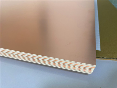
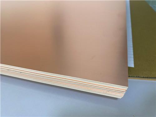
Figure 1. Rogers RO4360G2 high-frequency laminate with copper foil cladding.
Conclusion (CCL)
RO4360G2 high frequency substrate sits between PTFE and FR-4: a high-Dk, low-loss hydrocarbon-ceramic thermoset that offers PTFE-like RF stability without PTFE handling cost. For this 12 mil, two-layer, ENEPIG power-amplifier board, it is the reason the product is both electrically demanding and economically producible on standard equipment.
If you have questions or suggestions,please leave us a message,we will reply you as soon as we can!
Categories
New Products
Wangling TF440 25mil DK4.4 Laminate Immersion Gold 2-Layer Copper-filling Vias PCB
RO4360G2 Rogers 12mil ENEPIG 2-Layer DK6.15 High Frequency Custom PCB
Wangling F4BTMS220 2-Layer DK2.2 PCB 10 mil Core with Immersion Gold
Wangling F4BTME350 10mil DK3.5 High Frequency Substrate PCB 2-Layer Immersion Gold
Wangling F4BTM300 Custom 2-layer PCB 20mil DK3.0 Substrate with Immersion Gold
Rogers 20mil RT/duroid 6202 2-layer ENIG High-Frequency Microwave PCB
Rogers 20mil AD250C PCB Pure Gold High-Frequency Antenna Circuit Board
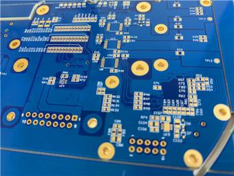
8-Layer Hybrid RF PCB: RO4350B + TG170 FR-4 + RO4003C with RO4450F Bondply
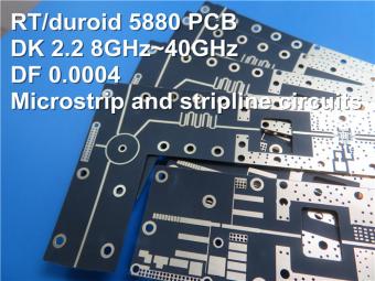
This is a type of double sided RF PCB built on RT/duroid 5880 for the application of Radar Systems.
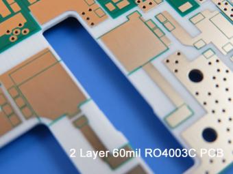
RO4003C PCBs are hydrocarbon ceramic filled laminates, not PTFE which are designed to offer superior high frequency performance.
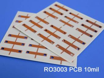
Rogers RO3003 high frequency circuit materials are ceramic-filled PTFE composites intended for use in commercial microwave and RF applications. It was designed to offer exceptional electrical and mechanical stability at competitive prices.
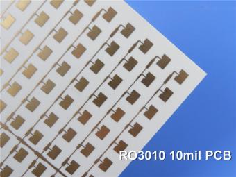
RO3010 laminates are competitively priced products with exceptional mechanical and electrical stability. This stability simplifies the design of broadband components and allows the materials to be used in a wide range of applications over a very broad range of frequencies.
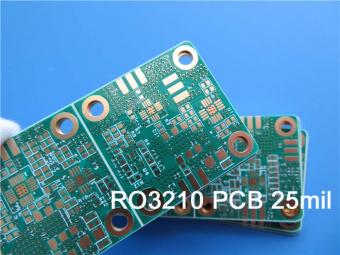
These RO3210 materials are engineered to offer exceptional electrical performance and mechanical stability. RO3210 laminates combine the surface smoothness of a non-woven PTFE laminate.
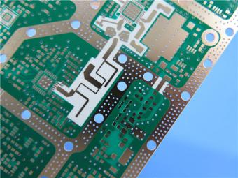
RT/duroid 6035HTC laminates are an exceptional choice for high power applications.
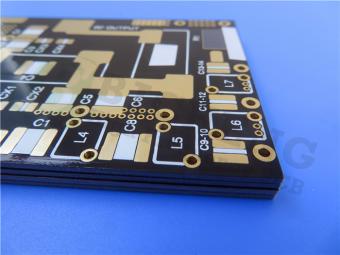
TC350 is designed to provide enhanced heat-transfer through “Best-In-Class” thermal conductivity, while reducing dielectric loss and insertion loss. Lower losses result in higher Amplifier and Antenna Gains/Efficiencies.
RO3035 materials exhibit a coefficient of thermal expansion(CTE) in the X and Y axis of 17 ppm/℃. This expansion coefficient is matched to that of copper, which allows the material to exhibit excellent dimensional stability.
 6-11C Shidai Jingyuan, Fuyong, Baoan, Shenzhen, Guangdong, China 518103


For inquiries about our products or pricelist, please leave to us and we will be in touch within 24 hours.
© Copyright: 2026 Shenzhen Bicheng Electronics Technology Co., Ltd.. All Rights Reserved.

IPv6 network supported


