

 Call Us Now !
Tel : +86 755 27374946
Call Us Now !
Tel : +86 755 27374946
 Order Online Now !
Email : info@bichengpcb.com
Order Online Now !
Email : info@bichengpcb.com
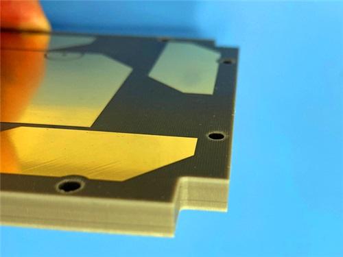
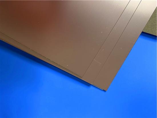
F4BM233 is a well-characterized, production-proven PTFE-glass high-frequency laminate that combines a tightly controlled Dk of 2.33 (±0.04) with low dissipation factor (0.0011 at 10 GHz), broad operating temperature range (−55 °C to +260 °C), and UL 94 V-0 flammability.
Item NO.:
BIC-620-v705Order(MOQ):
1-10Payment:
T/TProduct Origin:
ChinaShipping Port:
ShenzhenLead Time:
7-10 days
2-Layer F4BM233 4.0mm Wangling Substrate High-Frequency Custom PCB with ENIG Finish
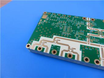
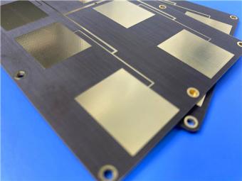
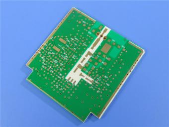
This PCB is a double-sided high-frequency circuit board built on F4BM233 PTFE-glass composite laminate, with a finished board thickness of 4.0 mm and 1 oz (35 µm) copper on both outer layers.
The 4.0 mm Wangling substrate thickness is a deliberate engineering choice. It elevates the board's natural rigidity, reduces flex-induced microstrip impedance drift, and supports wider conductor widths for a given target impedance compared with thin laminates. These properties make the F4BM DK2.33 board particularly well suited for power-handling RF circuits, antenna feed networks, and test fixtures where dimensional stability under thermal cycling is critical to long-term performance repeatability. The ENIG finish further ensures that connector mating surfaces remain flat and solderable through multiple reflow cycles, an important consideration for boards that may be assembled, reworked, or field-serviced over an extended service life.
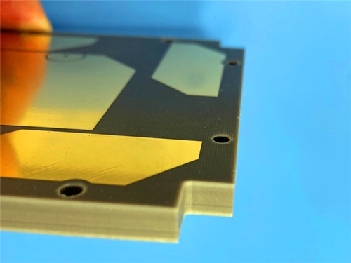
· Low-loss dielectric core — F4BM233 offers a typical dielectric constant (Dk) of 2.33 at 10 GHz with a tight tolerance of ±0.04, and a dissipation factor (Df) of 0.0011 at 10 GHz (0.0015 at 20 GHz), keeping insertion loss low across microwave bands.
· Thick, rigid construction — the 4.0 mm finished thickness provides exceptional flatness and mechanical stability, with an in-plane coefficient of thermal expansion (CTE) of 22–30 ppm/°C over −55 °C to +288 °C.
· ENIG surface finish — electroless nickel / immersion gold offers a planar surface ideal for fine-pitch components and RF connectors, with excellent shelf life and wire-bonding compatibility.
· Asymmetric mask configuration — the top-side green solder mask protects component-side circuitry, while the bare bottom side is suited for ground-plane coupling, direct heat dissipation, or cavity mounting.
The table below summarizes the complete construction specification, from material selection and layer count through surface finish and outgoing quality control.
Table 1. PCB Construction Details
|
Parameter |
Specification |
|
Base material |
F4BM233 (PTFE + glass cloth) |
|
Layer count |
Double sided (2 layers) |
|
Board dimensions |
65 mm × 72 mm = 1 PCS, ±0.15 mm |
|
Minimum trace / space |
Per design files |
|
Minimum hole size |
Per design files |
|
Blind / buried vias |
No blind vias |
|
Finished board thickness |
4.0 mm |
|
Finished Cu weight |
1 oz (1.4 mils / 35 µm) outer layers |
|
Via plating thickness |
Per design files |
|
Surface finish |
Immersion Gold (ENIG) |
|
Top silkscreen |
No |
|
Bottom silkscreen |
No |
|
Top solder mask |
Green |
|
Bottom solder mask |
No |
|
Electrical test |
100 % electrical test prior to shipment |
The cross-sectional stackup reflects a symmetric two-layer build on a single F4BM233 core, with 1 oz copper on both outer layers and a green solder mask applied only to the top side. The dielectric core accounts for approximately 3.93 mm of the total 4.0 mm finished thickness.
Table 2. PCB Cross-Sectional Stackup
|
Layer |
Material |
Thickness |
Description |
|
Top Solder Mask |
Green LPI |
~15–25 µm |
Top side only; no silkscreen |
|
Layer 1 (Top) |
Copper (ED foil) |
35 µm (1 oz) |
Signal / component layer; ENIG finished |
|
Core Dielectric |
F4BM233 (PTFE + glass cloth) |
~3.93 mm |
Dk 2.33 @ 10 GHz; Df 0.0011 |
|
Layer 2 (Bottom) |
Copper (ED foil) |
35 µm (1 oz) |
Ground / secondary signal; bare copper; ENIG finished |
|
Bottom Solder Mask |
None |
0 µm |
No mask; no silkscreen |
|
Total |
— |
4.0 mm |
Finished board thickness |
· Microwave and RF power amplifiers
· Antenna feed networks and phased-array antenna elements
· Power dividers, directional couplers, and combiners
· Phase shifters and passive RF components
· Satellite communication and base-station antenna modules
· High-frequency test fixtures and interposers
This 2-layer F4BM233 PCB combines a low-loss, tightly toleranced PTFE-glass dielectric with a robust 4.0 mm thick construction and ENIG surface finish, creating a platform that balances microwave electrical performance with mechanical durability. The asymmetric solder-mask configuration — green mask on top, bare copper on bottom — offers design flexibility for grounding, thermal management, and cavity integration. With 100 % electrical testing before shipment, the board is ready for integration into demanding RF and microwave subsystems where signal integrity, dimensional stability, and long-term reliability are non-negotiable.
Part 2 — CCL Material Knowledge: F4BM233
Wangling F4BM233 is a PTFE (polytetrafluoroethylene) glass-cloth copper-clad laminate (CCL) manufactured by Taizhou Wangling Insulation Materials Factory. It is produced by scientifically compounding glass cloth, PTFE resin, and PTFE film, then laminating under strictly controlled temperature and pressure conditions. Compared with the earlier F4B generation, the F4BM series delivers a wider selectable dielectric-constant range, lower dielectric loss, higher insulation resistance, and improved long-term stability, making it a commercially mature alternative to comparable imported high-frequency laminates.
The F4BM and F4BME variants share an identical dielectric layer but differ in the copper foil employed. F4BM uses standard electrodeposited (ED) copper foil and is intended for applications without passive-intermodulation (PIM) requirements. F4BME pairs the same dielectric with reversed-treated (RTF) copper foil, yielding superior PIM performance, tighter line-width control, and lower conductor loss. By adjusting the ratio of PTFE to glass cloth, the dielectric constant can be precisely tuned across the series; higher Dk grades contain proportionally more glass, which improves dimensional stability, lowers CTE, and enhances temperature drift characteristics at the expense of a slightly higher dissipation factor. The numeric suffix "233" denotes a typical Dk of 2.33.
· Dielectric constant selectable from 2.17 to 3.0, with custom Dk available on request
· Low dissipation factor across microwave frequency bands
· F4BME variant with RTF copper foil for excellent PIM (≤ −159 dBc)
· Multiple standard and custom panel sizes for cost optimization
· Radiation-resistant and low-outgassing, suitable for aerospace and high-vacuum environments
· Commercially mature, high-volume production with competitive cost-performance ratio
The following table presents the fullF4BM233 datasheet, covering electrical, thermal, mechanical, and environmental properties under their specified test conditions. Dielectric constant is measured in the Z-direction using the stripline method per GB/T 12636-1990 or IPC-TM-650 2.5.5.5; all other properties follow IPC-TM-650 or GB/T 4722-2017 test methods.
Table 3. F4BM233 Complete Datasheet
|
Property |
Test Condition |
Unit |
F4BM233 Value |
|
Dielectric Constant (typical) |
10 GHz |
— |
2.33 |
|
Dk Tolerance |
— |
— |
±0.04 |
|
Dissipation Factor (typical) |
10 GHz |
— |
0.0011 |
|
Dissipation Factor (typical) |
20 GHz |
— |
0.0015 |
|
Dk Temperature Coefficient |
−55 °C to 150 °C |
ppm/°C |
−130 |
|
Peel Strength (F4BM, 1 oz) |
1 oz ED foil |
N/mm |
>1.8 |
|
Peel Strength (F4BME, 1 oz) |
1 oz RTF foil |
N/mm |
>1.6 |
|
Volume Resistivity |
Normal condition |
MΩ·cm |
≥6×10⁶ |
|
Surface Resistivity |
Normal condition |
MΩ |
≥1×10⁶ |
|
Electric Strength (Z-dir.) |
5 kW, 500 V/s |
kV/mm |
>23 |
|
Breakdown Voltage (XY-dir.) |
5 kW, 500 V/s |
kV |
>32 |
|
CTE (XY-direction) |
−55 °C to 288 °C |
ppm/°C |
22–30 |
|
CTE (Z-direction) |
−55 °C to 288 °C |
ppm/°C |
205 |
|
Thermal Stress |
260 °C, 10 s, 3 cycles |
— |
No delamination |
|
Water Absorption |
20±2 °C, 24 h |
% |
≤0.08 |
|
Density |
Room temperature |
g/cm³ |
2.20 |
|
Continuous Use Temperature |
High/low temp chamber |
°C |
−55 to +260 |
|
Thermal Conductivity |
Z-direction |
W/(m·K) |
0.28 |
|
PIM Value (F4BME only) |
— |
dBc |
≤−159 |
|
Flammability |
— |
UL-94 |
V-0 |
|
Material Composition |
— |
— |
PTFE + glass cloth; F4BM = ED foil, F4BME = RTF foil |
F4BM (ED copper) is available in foil thicknesses of 0.5 oz (0.018 mm), 1 oz (0.035 mm), 1.5 oz (0.05 mm), and 2 oz (0.07 mm). F4BME (RTF copper) supports 0.5 oz and 1 oz options.
Standard panel sizes include 460×610 mm, 500×600 mm, 850×1200 mm, 914×1220 mm, and 1000×1200 mm; custom sizes such as 300×250 mm, 350×380 mm, 500×500 mm, 840×840 mm, and 1000×1500 mm are available on request.
An important manufacturing constraint applies: when the laminate thickness is ≥4.0 mm or ≤0.2 mm, the panel size must not exceed 500×610 mm.
The material is offered in a broad range of dielectric thicknesses from 0.1 mm to 12.0 mm, with thickness tolerances tightening for thinner gauges (±0.01 mm at 0.1 mm) and widening for thicker sections (±0.20 mm at 12.0 mm). At 4.0 mm, the standard thickness tolerance is ±0.10 mm.
Customers should specify whether the quoted thickness refers to the total copper-clad thickness or the dielectric thickness alone when placing an order. For the 4.0 mm PCB described in Part 1, this thickness sits at the threshold where panel size is restricted to 500×610 mm or smaller, a factor that influences production panelization and per-unit cost.
Beyond standard double-sided CCL, the F4BM / F4BME platform is also available in metal-backed configurations where the dielectric layer is clad with copper foil on one side and bonded to an aluminum or copper metal base on the other. These variants — designated F4BM-AL, F4BME-AL, F4BM-CU, and F4BME-CU — provide electromagnetic shielding and enhanced heat dissipation, making them suitable for high-power RF modules and thermal-critical designs.
Table 4. Metal-Backed CCL Variants
|
Model |
Metal Base |
Density (g/cm³) |
Thermal Cond. (W/m·K) |
Base Thickness (mm) |
Panel Size (mm) |
|
F4BM-CU |
Copper (purple / brass) |
8.9 |
380 |
0.48–3.98 |
460×610, 460×305 |
|
F4BME-CU |
Copper (purple / brass) |
8.9 |
380 |
0.48–3.98 |
460×610, 460×305 |
|
F4BM-AL |
Aluminum |
2.7 |
180 |
0.48–3.98 |
460×610, 460×305 |
|
F4BME-AL |
Aluminum |
2.7 |
180 |
0.48–3.98 |
460×610, 460×305 |
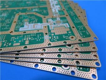
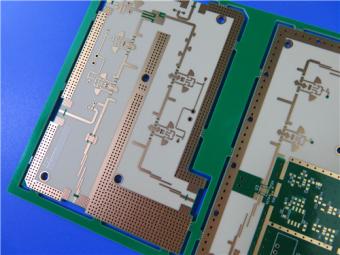
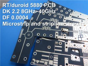
The image below illustrates representative high-frequency circuit boards fabricated on F4BM-series laminates, including microstrip feed networks, circular antenna elements, and multi-channel RF modules — demonstrating the material's versatility across microwave and antenna applications.
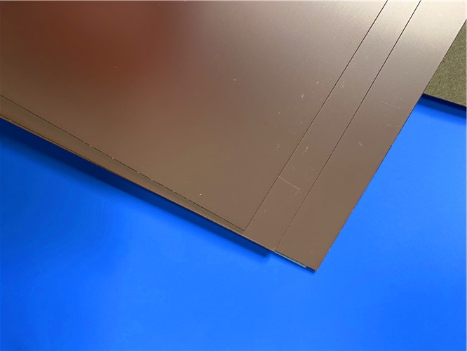
Figure 1. Representative RF/microwave PCBs built on F4BM-series laminates.
F4BM233 is a well-characterized, production-proven PTFE-glass high-frequency laminate that combines a tightly controlled Dk of 2.33 (±0.04) with low dissipation factor (0.0011 at 10 GHz), broad operating temperature range (−55 °C to +260 °C), and UL 94 V-0 flammability. Its availability in multiple copper-foil types (ED and RTF), thicknesses from 0.1 mm to 12.0 mm, and metal-backed variants (aluminum or copper base) provides engineers with significant design flexibility.
For the 4.0 mm double-sided ENIG Wangling PCB described in Part 1, F4BM233 supplies the dielectric foundation that enables consistent impedance control, low insertion loss, and mechanical robustness — making it a sound choice for microwave, radar, satellite, and base-station applications where material consistency directly translates to system-level performance.
Previous:
Wangling TP2200 PCB 0.8mm Substrate Immersion Gold 2-Layer High-Dk (Dk 22) RF BoardNext:
Wangling TF960 Custom PCB High DK 9.6 Laminate 0.635mm Immersion Silver FinishIf you have questions or suggestions,please leave us a message,we will reply you as soon as we can!
Categories
New Products
10-Layer RO4350B + TU-768 Hybrid PCB with Via Copper Capped ENIG Surface Finish
8-Layer 6.6mil Rogers RO4350B + Isola I-Tera MT40 Hybrid PCB 1.636mm Pressed Thickness ENEPIG
6-Layer 5mil Rogers RO3003 Mixed-Laminated with Isola 370HR 0.82 mm Hybrid PCB with ENIG
4-Layer 8mil RO4003C + Tg170 FR-4 Hybrid PCB with ENIG — 0.556mm Thin Build
1100 × 350mm Long-Format Rogers RO4003C 32 mil core Double-Sided High-Frequency PCB
Wangling TP2200 PCB 0.8mm Substrate Immersion Gold 2-Layer High-Dk (Dk 22) RF Board
Rogers TMM10 PCB 5.08mm Core ENIG 2-Layer High-Dk Microwave Board
Taconic TLX-8 PCB 50mil ENIG 2-Layer High-Frequency RF Circuit Board

RF-10 25mil Taconic PCB Materials stands out as a high-performance solution for RF applications. Its exceptional electrical properties, dimensional stability, thermal conductivity, and adhesion characteristics make it an ideal choice for demanding applications.
The PCB has a 4-layer hybrid stackup with a 0.5oz+plating ground layer, two 1oz ground layers, and a 0.5oz+plating signal layer.
The dimensions of the board are 55.00 x 26.00 mm, with a tolerance of +/- 0.15mm. The board has 16 components, 26 total pads, 9 through-hole pads, 10 top SMT pads, 7 bottom SMT pads, 77 vias, and 82 nets.
Rogers RO4003C PCB is an innovative and advanced circuit board that is made with high-quality materials.
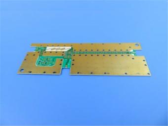
The RO4350B PCB offers a range of benefits that make it an ideal choice for high-frequency applications. Its low dielectric loss and high thermal conductivity make it perfect for high-frequency applications such as RF and microwave circuits.

Bicheng PCB Ships High-Quality PCBs with Shengyi Tg150 ℃ S1000H Material and Advanced Stackup
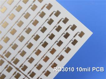
Rogers RO3010 PCB is ideal for a wide range of high-frequency applications, including power amplifiers, filters, couplers, and antennas.
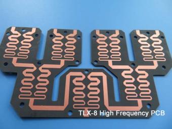
TLX-8 features low dielectric loss, low moisture absorption, and excellent thermal stability, making it ideal for high-frequency and high-speed applications. It has a low dissipation factor, which helps to minimize signal loss and distortion.
 6-11C Shidai Jingyuan, Fuyong, Baoan, Shenzhen, Guangdong, China 518103


For inquiries about our products or pricelist, please leave to us and we will be in touch within 24 hours.
© Copyright: 2026 Shenzhen Bicheng Electronics Technology Co., Ltd.. All Rights Reserved.

IPv6 network supported


