

 Call Us Now !
Tel : +86 755 27374946
Call Us Now !
Tel : +86 755 27374946
 Order Online Now !
Email : info@bichengpcb.com
Order Online Now !
Email : info@bichengpcb.com
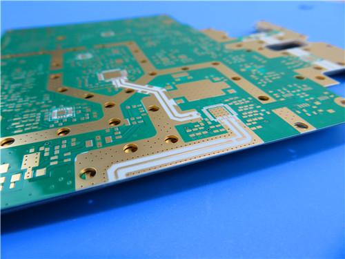
This 6-layer RO4003C TG170 FR4 mixed dielectric PCB establishes a balanced high-reliability RF-digital hybrid circuit solution, breaking the single-material performance-cost tradeoff limitation of traditional multi-layer PCBs.
Item NO.:
BIC-583-v668.0Order(MOQ):
1-10Payment:
T/TProduct Origin:
ChinaShipping Port:
ShenzhenLead Time:
7-10 days
6-Layer RO4003C + FR4 Mixed Dielectric PCB with Hard Gold Plating Blind Via
Product Overview
The 6-Layer Hybrid PCB represents a sophisticated engineering solution that combines the exceptional high-frequency performance of Rogers RO4003C hydrocarbon ceramic laminates with the cost-effectiveness and mechanical robustness of FR-4 materials. This innovative mixed dielectric construction addresses the growing industry demand for printed circuit boards that can handle both high-speed digital signals and RF/microwave frequencies while maintaining reliable performance across a wide range of operating conditions. The strategic material selection and layer arrangement demonstrate a deep understanding of signal integrity requirements, thermal management challenges, and manufacturing practicality in modern electronic systems.
This product has been specifically engineered for applications requiring controlled impedance transmission lines, superior high-frequency performance, and reliable operation in demanding environments. The integration of RO4003C material in the core layer provides outstanding dielectric properties, while the TG170°C FR-4 materials ensure structural stability and cost-effective manufacturing. The board achieves a finished thickness of 1.74mm with 1oz copper on all layers, supporting both blind via structures and comprehensive impedance control requirements
1. Product Core Positioning & Differentiated Design Logic
Traditional single-material multi-layer PCBs face obvious application bottlenecks: full RO4003C 6-layer boards bring excessive raw material cost and complicated lamination process control; pure TG170 FR4 6-layer boards fail to meet low-loss, tight impedance requirements for RF/microwave transmission lines at 1–10 GHz frequency bands. Thishybrid 6-layer PCB adopts a targeted material partitioning architecture: L1 and L6 outer signal layers adoptRogers RO4003C low-loss dielectricfor high-frequency trace routing, while L2–L5 inner layers use TG170 FR4 core + matched TG170 FR4 prepreg as the medium layer. This design achieves three core differentiated competitive edges:
1.1 Electrical differentiation:
Outer high-frequency traces maintain Dk=3.38±0.05, Df=0.0027@10GHz ultra-low signal attenuation, eliminating phase shift and insertion loss drift of ordinary FR4 (Dk≈4.3, Df≈0.022@10GHz);
1.2 Cost & manufacturability differentiation:
Central FR4 core replaces expensive full Rogers medium, compatible with standard FR4 lamination, drilling, plating production lines without special PTFE processing equipment;
1.3 Thermal reliability differentiation:
Dual high-Tg materials (RO4003C Tg>280℃, FR4 Tg=170℃) jointly resist thermal shock during reflow, soldering dip and long-term high-temperature operation, supporting IPC-3 high-reliability aerospace, automotive radar, industrial wireless communication scenarios.
The finished board adopts hard electrolytic gold plating as surface finish, L1-L2 & L5-L6 sequential blind vias for high-density interconnection, full-layer 1oz copper, 25μm uniform via copper plating, strict impedance control, and 100% full-net electrical testing before delivery, fully compliant with IPC-3 Class 3 high-performance PCB acceptance criteria.
2. PCB Complete Construction Details
The table below summarizes all fixed dimensional, material, surface treatment, testing and standard specifications of this hybrid 6-layer PCB, with unified tolerance and thickness control parameters for mass production consistency.
| Parameter | Specification |
| Base Material | RO4003C + TG170°C FR4 PP + TG170°C FR4 |
| Layer Count | 6 layers |
| Board Dimensions | 127mm x 103mm = 1PCS (Including process edge) |
| Blind Vias | L1-L2, L5-L6 |
| Finished Board Thickness | 1.74mm |
| Finished Cu Weight | 1oz (1.4 mils) for all layers |
| Via Plating Thickness | 25 μm |
| Surface Finish | Hard Electrolytic Gold Plating |
| Top Silkscreen | White legend |
| Bottom Silkscreen | White legend |
| Top Solder Mask | Green solder mask |
| Bottom Solder Mask | Green solder mask |
| Standard | IPC-3 |
| Impedance Control | Required |
| Electrical Test | 100% Electrical test used prior to shipment |
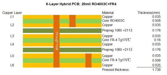
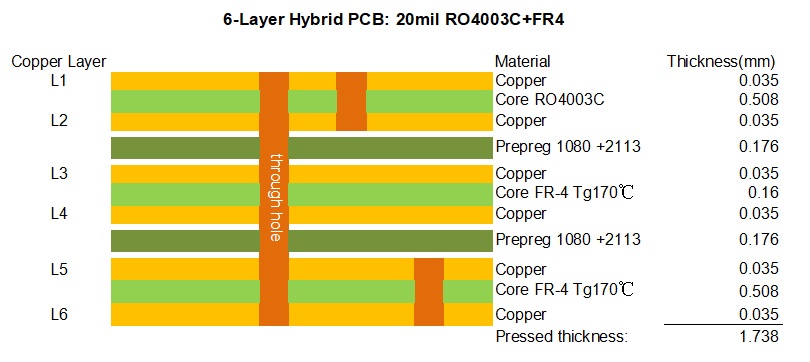
3. Optimized 6-Layer Mixed Dielectric PCB Stackup
This stackup adopts symmetric dielectric layout to eliminate board warpage during lamination and thermal cycling, placing Rogers 4003C on outer signal layers and TG170 FR4 core in the center to balance RF performance and thermal-mechanical stability.
Stackup sequence from Top Layer L1 to Bottom Layer L6, total finished thickness 1.74mm:
4. Key Manufacturing & Performance Differentiation Analysis
4.1 Blind Via Design Value (L1-L2, L5-L6)
Sequential blind vias replace full through vias on outer RF layers, avoiding via stub parasitic inductance that distorts high-frequency impedance. The 25μm uniform barrel plating ensures stable current carrying capacity for RF power signals, and paired with 1oz full-layer copper, minimizes DC resistance loss of transmission lines. For IPC-3 high-reliability demand, all blind via holes undergo resin filling and planarization to eliminate voids during thermal cycling.
4.2 Hard Electrolytic Gold Plating Surface Finish Advantages
Different from immersion gold (ENIG) ultra-thin chemical gold (0.05μm typical), IPC-3 grade hard electrolytic cobalt-alloy gold reaches minimum 1.25μm gold thickness with 2.5μm nickel diffusion barrier underneath. Hard gold hardness reaches 160–190 HV, resisting thousands of connector plug-in cycles without abrasion, maintaining stable low contact resistance (<20mΩ) in long-term high-frequency signal transmission. The nickel barrier completely blocks copper ion diffusion to gold surface, preventing oxidation and contact resistance drift under high-temperature humidity aging (85℃/85%RH, 1000hrs). Green solder mask covers all non-contact areas, white silkscreen provides clear component polarity marking without RF signal interference.
4.3 Impedance Control & Electrical Stability
RO4003C outer layers deliver fixed Dk=3.38±0.05 across 1–10GHz frequency bands, eliminating the dielectric constant frequency drift defect of standard FR4. The symmetric stackup structure ensures consistent trace width calculation for single-ended and differential impedance, with production impedance testing using TDR time-domain reflectometer to verify all critical RF traces before electrical test. Full 100% flying probe electrical test eliminates open/short circuit risks of multi-layer interconnection blind vias, complying with IPC-3 zero critical defect delivery standard.

4.4 Thermal & Mechanical Reliability
The dual high-Tg mixed dielectric system solves the thermal mismatch problem between ordinary FR4 and microwave materials. RO4003C Td thermal decomposition temperature 425℃, TG170 FR4 passes 288℃10-second solder dip without delamination; low Z-axis CTE of RO4003C (46ppm/℃) offsets higher FR4 Z-expansion, reducing layer separation risk during repeated reflow cycles. The±0.15mm dimensional tolerance controls board deformation during mass lamination, suitable for automated SMT assembly.
5. PCB Product Conclusion
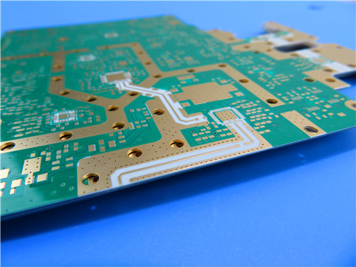
This 6-layer RO4003C TG170 FR4 mixed dielectric PCB establishes a balanced high-reliability RF-digital hybrid circuit solution, breaking the single-material performance-cost tradeoff limitation of traditional multi-layer PCBs. The layered material partition design precisely allocates low-loss microwave medium to high-frequency signal transmission areas and cost-effective high-Tg FR4 to digital power/ground inner layers, supported by symmetric stackup, controlled blind vias, IPC-3 hard gold surface finish, full-layer uniform copper and 100% electrical testing.
Its core differentiated strengths include stable ultra-low high-frequency loss, excellent thermal shock resistance, lower manufacturing cost than full-Rogers multi-layer boards, and plug-in wear-resistant hard gold contact surfaces, widely applicable to automotive millimeter-wave radar, industrial wireless transceivers, IoT high-frequency sensor modules and aerospace lightweight communication control boards. All structural, electrical and dimensional parameters are fully quantifiable and repeatable for mass production, with complete test verification standards to guarantee long-term service life under harsh operating environments.
CCL Raw Material In-Depth Technical Explanation
1. CCL System Overview of This Hybrid PCB
The finished PCB relies on two core copper clad laminate raw materials: Rogers RO4003C hydrocarbon ceramic high-frequency CCL and domestic TG170 lead-free high-Tg FR4 epoxy glass CCL, plus matched TG170 FR4 bonding prepreg. This section independently elaborates raw material composition, full datasheet parameter table, material structure characteristics, processing compatibility and application boundaries, without overlapping finished PCB manufacturing content.
2. Rogers RO4003C High-Frequency CCL Complete Datasheet Table
Material Base Composition: Woven glass reinforced hydrocarbon resin filled with ceramic powder, non-PTFE microwave laminate, compatible with standard FR4 PCB fabrication lines
| Property | Typical Value | Tolerance / Condition | Units | Test Method |
| Dielectric Constant (εᵣ) Process | 3.38 | ±0.05 @ 10GHz/23°C | — | IPC-TM-650 2.5.5.5 (Clamped Stripline) |
| Design Dk (8-40 GHz) | 3.55 | Average | — | Differential Phase Length |
| Dissipation Factor (tan δ) | 0.0027 | @ 10 GHz / 23°C | — | IPC-TM-650 2.5.5.5 |
| Thermal Coefficient of εᵣ | 40 | -50°C to 150°C | ppm/°C | IPC-TM-650 2.5.5.5 |
| Volume Resistivity | 1.7×10¹⁰ | COND A | MΩ·cm | IPC-TM-650 2.5.17.1 |
| Surface Resistivity | 4.2×10⁹ | COND A | MΩ | IPC-TM-650 2.5.17.1 |
| Electrical Strength | 31.2 (780) | 0.51mm thickness | kV/mm (V/mil) | IPC-TM-650 2.5.6.2 |
| Tensile Modulus (X) | 19,650 (2,850) | RT | MPa (ksi) | ASTM D638 |
| Tensile Modulus (Y) | 19,450 (2,821) | RT | MPa (ksi) | ASTM D638 |
| Coefficient of Thermal Expansion (X) | 11 | -55 to 288°C | ppm/°C | IPC-TM-650 2.4.41 |
| Coefficient of Thermal Expansion (Y) | 14 | -55 to 288°C | ppm/°C | IPC-TM-650 2.4.41 |
| Coefficient of Thermal Expansion (Z) | 46 | -55 to 288°C | ppm/°C | IPC-TM-650 2.4.41 |
| Tg (TMA) | >280 | — | °C | IPC-TM-650 2.4.24.3 |
| Td (5% weight loss) | 425 | — | °C | ASTM D3850 |
| Thermal Conductivity | 0.71 | @ 80°C | W/m·K | ASTM C518 |
| Moisture Absorption | 0.06 | 48 hrs immersion | % | ASTM D570 |
| Density | 1.79 | @ 23°C | g/cm³ | ASTM D792 |
| Copper Peel Strength | 1.05 (6.0) | after solder float | N/mm (pli) | IPC-TM-650 2.4.8 |
| Flammability | N/A | (Non-UL rated for FR) | — | UL 94 |
| Lead-Free Process Compatible | Yes | — | — | — |
RO4003C CCL Structural & Processing Feature Description
Unlike PTFE microwave substrates requiring special etching, drilling and lamination processes, RO4003C uses thermosetting hydrocarbon resin matrix, which can be laminated, drilled, plated and etched on standard FR4 production equipment without dedicated fluoropolymer processing lines. The ceramic filler uniformly dispersed in the resin matrix stabilizes dielectric constant across wide frequency bands, eliminating Dk fluctuation of glass fiber woven substrates at high GHz frequency. Its main limitation is lack of UL94 V-0 flame retardant rating, so it must be compounded with V-0 certified TG170 FR4 CCL/prepreg for complete flame resistance of the finished PCB, which forms the core reason for this mixed dielectric design.
TG170 FR4 CCL Application & Matching Logic
This FR4 CCL and its matched prepreg act as the central core and bonding medium of the hybrid PCB, solving two critical defects of pure RO4003C boards: UL94 V-0 flame retardancy and cost control. The high Tg 170℃characteristic fully adapts to lead-free SMT reflow temperature curves, resisting interlayer separation during lamination with RO4003C. Its higher copper peel strength provides reliable adhesion for inner power/ground large copper planes, while low water absorption suppresses CAF failure in long-term high-humidity operation. Due to higher Df loss tangent, it is only arranged in inner digital layers without high-frequency RF traces, avoiding signal attenuation defects.
4. CCL Material Matching Principle for This 6-Layer Hybrid PCB
The co-lamination of RO4003C and TG170 FR4 relies on identical thermal lamination pressure and temperature window of the two resin systems, which avoids interlayer voids and warpage during pressing. The symmetric layout of RO4003C on L1 and L6 outer layers balances thermal expansion stress, and the central thick TG170 FR4 core provides mechanical rigidity for the whole board. The supporting TG170 FR4 prepreg serves as the bonding medium between RO4003C outer core and inner FR4 copper layers, forming a continuous compatible resin interface without delamination risk.
5. CCL Raw Material Conclusion
The dual-CCL mixed dielectric system of RO4003C high-frequency microwave laminate and TG170 lead-free high-Tg FR4 laminate is the core technical foundation of this 6-layer PCB. RO4003C delivers industry-leading low-loss, tight Dk tolerance electrical performance for outer RF transmission circuits, while TG170 FR4 supplies flame retardancy, low manufacturing cost and outstanding thermal-mechanical stability for inner digital power circuits.
The two materials have complementary performance advantages and compatible fabrication processes, eliminating the single material performance bottleneck and forming a cost-effective high-reliability hybrid substrate solution for RF-digital integrated multi-layer PCBs.
All datasheet parameters cited in this chapter are sourced from official Rogers RO4003C material specifications and IPC-certified TG170 FR4 CCL manufacturer test reports, with accurate, repeatable engineering data to support stackup design and mass production quality control.
Previous:
4-Layer Wangling WL-CT338 + FR4 Hybrid PCB ENIG Green Solder Mask White SilkscreenNext:
10-Layer Rogers RO4003C + 370HR FR4 Hybrid Laminate PCB ENIG Impedance ControlIf you have questions or suggestions,please leave us a message,we will reply you as soon as we can!
Categories
New Products
Wangling F4BTMS220 2-Layer DK2.2 PCB 10 mil Core with Immersion Gold
Wangling F4BTME350 10mil DK3.5 High Frequency Substrate PCB 2-Layer Immersion Gold
Wangling F4BTM300 Custom 2-layer PCB 20mil DK3.0 Substrate with Immersion Gold
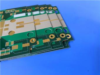
Rogers 20mil RT/duroid 6202 2-layer ENIG High-Frequency Microwave PCB
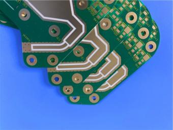
Rogers 20mil AD250C PCB Pure Gold High-Frequency Antenna Circuit Board
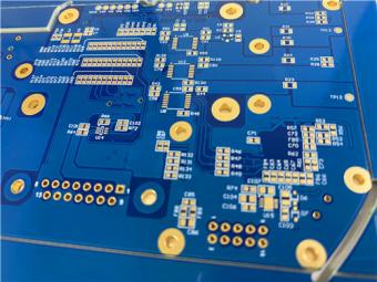
8-Layer Hybrid RF PCB: RO4350B + TG170 FR-4 + RO4003C with RO4450F Bondply
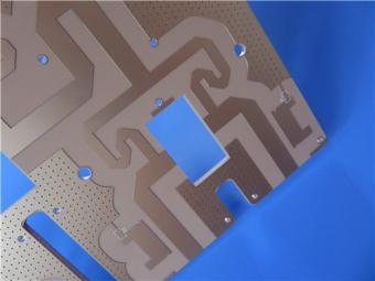
4-Layer Rogers RO3010 Hybrid PCB Immersion Silver 2.8mm Finished Thickness
4-Layer 20mil Rogers RO3210 ISIG High-Frequency PCB with Controlled Depth Milling
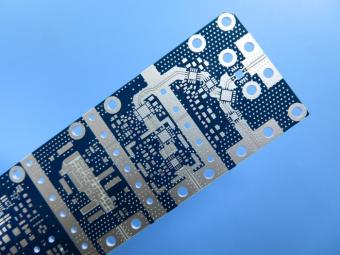
RO4003C exhibit a stable dielectric constant over a broad frequency range. This makes it an ideal substrate for broadband applications. And signal integrity performance improvement over the stack-ups with all FR4 board.
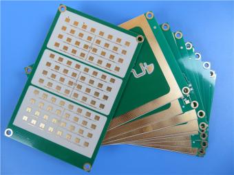
The hybrid PCB can be a mixture of FR-4 and high frequency material, and a mixture of high frequency material with different dielectric constant (DK)
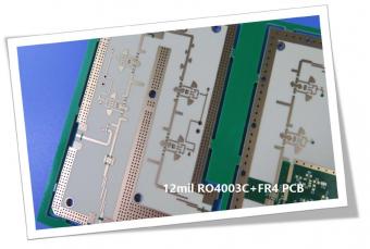
The 12mil core is on the top layer and it mainly plays the roles of signal layer. The core has fixed thickness which is very important to the electrical length of RF lines on the circuit board.
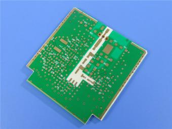
The hybrid PCB can be a mixture of FR-4 and high frequency material as abovementioned.
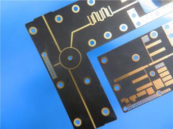
It contains 2 different boards in the panel. PCB boards are manufactured strictly as per required specifications with the standard IPC-Class-II.
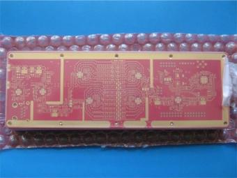
Hybrid PCB is also known as mixed material lamination, it’s normally combined by two different material like FR4 and PI(rigid flex PCB), FR4 and Ceramic, FR4 and Teflon, FR4 and Aluminum base etc.
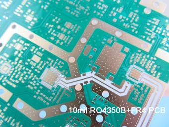
Hybrid constructions PCB typically involve a low loss material such as Nelco or Rogers combined with another core material like FR-4.
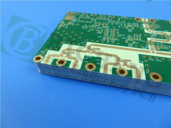
The Hybrid PCB on RO3003 and High Tg FR-4 is a state-of-the-art solution for high-frequency applications. With its exceptional stability, reliability, and manufacturability, it caters to the demands of industries such as automotive, telecommunications, and satellite communications.
 6-11C Shidai Jingyuan, Fuyong, Baoan, Shenzhen, Guangdong, China 518103


For inquiries about our products or pricelist, please leave to us and we will be in touch within 24 hours.
© Copyright: 2026 Shenzhen Bicheng Electronics Technology Co., Ltd.. All Rights Reserved.

IPv6 network supported


