

 Call Us Now !
Tel : +86 755 27374946
Call Us Now !
Tel : +86 755 27374946
 Order Online Now !
Email : info@bichengpcb.com
Order Online Now !
Email : info@bichengpcb.com
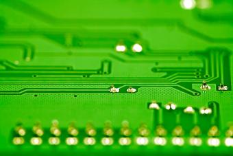
This 8-layer TC350 and FR408HR PCB integrates premium materials, optimized stackup design, and advanced manufacturing processes to deliver consistent performance, reliability, and adaptability for high-end electronic applications.
Item NO.:
BIC-541-v626.0Order(MOQ):
1-10Payment:
T/TProduct Origin:
ChinaShipping Port:
ShenzhenLead Time:
7-10 days
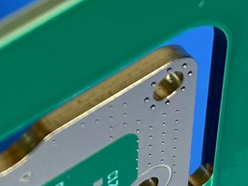
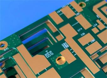
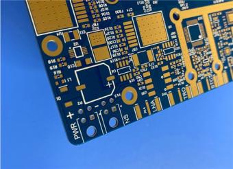
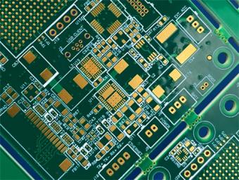
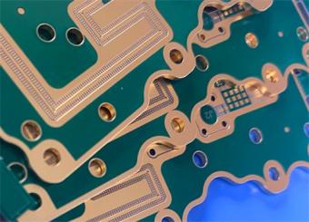
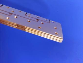
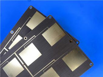
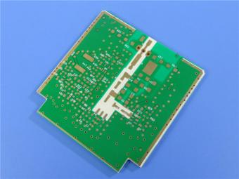
8-layer TC350 FR408HR Hybrid PCB with Blind Via Filled and Capped Edge Plating
Introducethis high-reliability 8-layer hybrid PCB, engineered with a hybrid material combination of TC350 laminate and FR408HR material to deliver exceptional thermal management, signal integrity, and mechanical stability. Designed for high-end electronic applications that demand precision, durability, and consistent performance, thishybridPCB integrates advanced manufacturing processes—including resin-filled and capped blind vias and metal edge plating—to meet the rigorous requirements of modern electronic systems. Below is a comprehensive overview of the product, including detailed construction specifications, stackup design, material insights, applications, and key technical explanations, with core data presented in tabular form for clarity.
PCB Construction Details
This summary outlines the core physical and manufacturing specifications of the 8-layer TC350 PCB, covering material, dimensions, copper weight, surface treatment, and quality control measures.
|
Construction Item |
Specification |
|
Material |
TC350 + FR408HR |
|
Layer Count |
8 layers |
|
Board Dimensions |
99mm x 83mm (per piece) |
|
Finished Board Thickness |
2.0mm |
|
Finished Cu Weight |
1oz (1.4 mils) for all layers |
|
Minimum Trace/Space |
4 / 4 mils |
|
Minimum Hole Size |
0.2mm (for blind vias) |
|
Blind Vias |
Yes, 0.2mm via filled and capped (resin filled and copper capped) |
|
Metal Edge Plating |
Yes |
|
Surface Finish |
Immersion Gold |
|
Top Silkscreen |
White |
|
Bottom Silkscreen |
White |
|
Top Solder Mask |
Green |
|
Bottom Solder Mask |
Green |
|
Quality Control |
100% Electrical test prior to shipment |
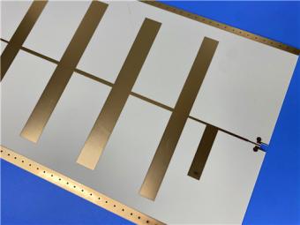
8-Layer PCB Stackup
The 8-layer PCB stackup is designed with symmetry to prevent board warpage, optimize signal integrity, and separate power and ground layers for enhanced electromagnetic compatibility (EMC), following industry best practices for high-performance multilayer PCBs.

Material Introduction: TC350 & FR408HR
TC350 and FR408HR are selected as the hybrid board material for this PCB, combining high thermal conductivity (TC350) and excellent thermal reliability (FR408HR) to meet diverse application demands.
- TC350: A high-performance PTFE composite material reinforced with glass cloth and ceramic filler, developed by Rogers Corporation. It features low insertion loss, high thermal conductivity (0.72 W/m-K), and stable dielectric constant (3.5±0.05 @ 10 GHz), making it ideal for high-frequency and high-power applications. Its low thermal expansion coefficient (7 ppm/°C in X/Y axis) ensures mechanical stability, while excellent copper adhesion enhances plating reliability. It is compatible with lead-free processes and offers superior thermal management to reduce component junction temperature.
- FR408HR: A high-performance FR-4 resin system from Isola Group, designed for multilayer PCBs requiring maximum thermal performance. With a glass transition temperature (Tg) of 190°C (DMA) and decomposition temperature (Td) of 360°C, it supports 6x 260°C reflow cycles and is CAF-resistant. It offers 30% improved Z-axis expansion and 25% more electrical bandwidth than competitive products, with excellent moisture resistance and compatibility with automated optical inspection (AOI) systems. It is RoHS-compliant and compatible with standard FR-4 manufacturing processes.

Data Sheet for TC350 & FR408HR
The following table summarizes the key technical parameters of RogersTC350 and FR408HR, providing critical data for design and manufacturing reference.
-TC350 Data Sheet
|
Typical Properties:TC350 |
|||
|
Property |
Units |
Value |
Test Merthod |
|
1. Electrical Properties |
|
||
|
Dielectric Constant (may vary by thickness) |
|
|
|
|
@1 MHz |
- |
3.50 |
IPC TM-650 2.5.5.3 |
|
@1.8 GHz |
- |
3.50 |
RESONANT CAVITY |
|
@10 GHz |
- |
3.50 |
IPC TM-650 2.5.5.5 |
|
Dissipation Factor |
|
|
|
|
@1 MHz |
- |
0.0015 |
IPC TM-650 2.5.5.3 |
|
@1.8 GHz |
- |
0.0018 |
RESONANT CAVITY |
|
@10 GHz |
- |
0.0020 |
IPC TM-650 2.5.5.5 |
|
Temperature Coefficient of Dielectric |
- |
|
|
|
TC r @ 10 GHz (-40-150°C) |
ppm/ºC |
-9 |
IPC TM-650 2.5.5.5 |
|
Volume Resistivity |
|
|
|
|
C96/35/90 |
MΩ-cm |
7.4x10⁶ |
IPC TM-650 2.5.17.1 |
|
E24/125 |
MΩ-cm |
1.4x10⁸ |
|
|
Surface Resistivity |
|
|
|
|
C96/35/90 |
MΩ |
3.2x10⁷ |
IPC TM-650 2.5.17.1 |
|
E24/125 |
MΩ |
4.3x10⁸ |
IPC TM-650 2.5.17.1 |
|
Electrical Strength |
Volts/mil (kV/mm) |
780 (31) |
IPC TM-650 2.5.6.2 |
|
Dielectric Breakdown |
kV |
40 |
IPC TM-650 2.5.6 |
|
Arc Resistance |
sec |
>240 |
IPC TM-650 2.5.1 |
|
2.Thermal Properties |
|
||
|
Decomposition Temperature (Td) |
|
|
|
|
Initial |
°C |
520 |
IPC TM-650 2.4.24.6 |
|
5% |
°C |
567 |
IPC TM-650 2.4.24.6 |
|
T260 |
min |
>60 |
IPC TM-650 2.4.24.1 |
|
T288 |
min |
>60 |
IPC TM-650 2.4.24.1 |
|
T300 |
min |
>60 |
IPC TM-650 2.4.24.1 |
|
Thermal Expansion, CTE (x,y) 50-150ºC |
ppm/ºC |
7, 7 |
IPC TM-650 2.4.41 |
|
Thermal Expansion, CTE (z) 50-150ºC |
ppm/ºC |
12 |
IPC TM-650 2.4.24 |
|
% z-axis Expansion (50-260ºC) |
% |
1.2 |
IPC TM-650 2.4.24 |
|
3. Mechanical Properties |
|
||
|
Peel Strength to Copper (1 oz/35 micron) |
|
|
|
|
After Thermal Stress |
lb/in (N/mm) |
7 (1.2) |
IPC TM-650 2.4.8 |
|
At Elevated Temperatures (150ºC) |
lb/in (N/mm) |
9 (1.6) |
IPC TM-650 2.4.8.2 |
|
After Process Solutions |
lb/in (N/mm) |
7 (1.2) |
IPC TM-650 2.4.8 |
|
Young’s Modulus |
kpsi (MPa) |
|
IPC TM-650 2.4.18.3 |
|
Flexural Strength (Machine/Cross) |
kpsi (MPa) |
14/10 (97/69) |
IPC TM-650 2.4.4 |
|
Tensile Strength (Machine/Cross) |
kpsi (MPa) |
11/8 (76/55) |
IPC TM-650 2.4.18.3 |
|
Compressive Modulus |
kpsi (MPa) |
|
ASTM D-3410 |
|
Poisson’s Ratio |
- |
|
ASTM D-3039 |
|
4. Physical Properties |
|
||
|
Water Absorption |
% |
0.05 |
IPC TM-650 2.6.2.1 |
|
Density, ambient 23ºC |
g/cm3 |
2.30 |
ASTM D792 Method A |
|
Thermal Conductivity |
W/mK |
0.72 |
ASTMD5470 |
|
Specific Heat |
J/gK |
0.90 |
ASTM D5470 |
|
Flammability |
class |
V0 |
UL-94 |
|
NASA Outgassing, 125ºC, ≤10- 6 torr |
|
|
|
|
Total Mass Loss |
% |
0.02 |
NASA SP-R-0022A |
|
Collected Volatiles |
% |
0.01 |
NASA SP-R-0022A |
|
Water Vapor Recovered |
% |
0.01 |
NASA SP-R-0022A |
-FR408HR Data Sheet
|
Property |
Typical Value |
Units |
Test Method |
|
|
|
|
Metric |
IPC-TM-650 (or as noted) |
|
|
Glass Transition Temperature (Tg) by DSC |
190 |
°C |
2.4.25C |
|
|
Decomposition Temperature (Td) by TGA @ 5% weight loss |
360 |
°C |
||
|
Time to Delaminate by TMA (Copper removed) |
A. T260 |
60 |
Minutes |
|
|
B. T288 |
>30 |
|||
|
Z-Axis CTE |
A. Pre-Tg |
55 |
ppm/°C |
2.4.24C |
|
B. Post-Tg |
230 |
ppm/°C |
||
|
C. 50 to 260°C, (Total Expansion) |
2.8 |
% |
||
|
X/Y-Axis CTE |
Pre-Tg |
16 |
ppm/°C |
2.4.24C |
|
Thermal Conductivity |
0.4 |
W/m·K |
ASTM E1952 |
|
|
Thermal Stress 10 sec @ 288ºC (550.4ºF) |
A. Unetched |
Pass |
Pass Visual |
|
|
B. Etched |
||||
|
Dk, Permittivity |
A. @ 100 MHz |
3.72 |
— |
2.5.5.3 |
|
B. @ 1 GHz |
3.69 |
2.5.5.9 |
||
|
C. @ 2 GHz |
3.68 |
Bereskin Stripline |
||
|
D. @ 5 GHz |
3.64 |
Bereskin Stripline |
||
|
E. @ 10 GHz |
3.65 |
Bereskin Stripline |
||
|
Df, Loss Tangent |
A. @ 100 MHz |
0.0072 |
— |
2.5.5.3 |
|
B. @ 1 GHz |
0.0091 |
2.5.5.9 |
||
|
C. @ 2 GHz |
0.0092 |
Bereskin Stripline |
||
|
D. @ 5 GHz |
0.0098 |
Bereskin Stripline |
||
|
E. @ 10 GHz |
0.0095 |
Bereskin Stripline |
||
|
Volume Resistivity |
A. After moisture resistance |
4.4 x 10⁷ |
M阝-cm |
|
|
B. At elevated temperature |
9.4 x 10⁷ |
|||
|
Surface Resistivity |
A. After moisture resistance |
2.6 x 10⁶ |
M阝 |
|
|
B. At elevated temperature |
2.1 x 10⁸ |
|||
|
Dielectric Breakdown |
>50 |
kV |
2.5.6B |
|
|
Arc Resistance |
137 |
Seconds |
2.5.1B |
|
|
Electric Strength (Laminate & laminated prepreg) |
70 (1741) |
kV/mm (V/mil) |
2.5.6.2A |
|
|
Comparative Tracking Index (CTI) |
2 (250-399) |
Class (Volts) |
UL 746A |
|
|
ASTM D3638 |
||||
|
Peel Strength |
A. Low profile copper foil and very low profile copper foil all copper foil >17阝m [0.669 mil] |
1.14 (6.5) |
N/mm (lb/inch) |
2.4.8C |
|
B. Standard profile copper |
||||
|
1. After thermal stress |
0.96 (5.5) |
2.4.8.2A |
||
|
2. After process solutions |
0.90 (5.1) |
2.4.8.3 |
||
|
Flexural Strength |
A. Length direction |
72.5 |
ksi |
2.4.4B |
|
B. Cross direction |
58 |
|||
|
Tensile Strength |
A. Length direction |
54.5 |
ksi |
ASTM D3039 |
|
B. Cross direction |
38.7 |
|||
|
Young's Modulus |
A. Length direction |
3695 |
ksi |
ASTM D790-15e2 |
|
B. Cross direction |
3315 |
|||
|
Poisson's Ratio |
A. Length direction |
0.137 |
— |
ASTM D3039 |
|
B. Cross direction |
0.133 |
|||
|
Moisture Absorption |
0.061 |
% |
2.6.2.1A |
|
|
Flammability (Laminate & laminated prepreg) |
V-0 |
Rating |
UL 94 |
|
|
Relative Thermal Index (RTI) |
130 |
°C |
UL 796 |
|
Applications
Leveraging its 8-layer design, hybrid PCB material advantages, and advanced manufacturing processes, this PCB is ideally suited for high-end electronic systems requiring high reliability, signal integrity, and thermal management. Key applications include:
- High-speed digital systems: Server motherboards, network switches/routers, high-end graphics cards, and AI acceleration cards.
- High-frequency communication equipment: 5G base stations, optical modules, microwave combiners, and power dividers.
- Industrial control systems: Precision industrial control motherboards, data acquisition cards, and automation equipment.
- Medical devices: High-reliability medical equipment motherboards (e.g., diagnostic instruments).
- Aerospace and automotive electronics: High-temperature, high-reliability electronic components (compliant with strict industry standards).
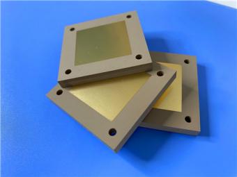
What is Via Filled and Capped (Resin Filled and Copper Capped)?
Via filled and capped (resin filled and copper capped) is an advanced PCB manufacturing process designed for high-density and high-reliability applications.
It involves two key steps: first, filling the blind vias (0.2mm in this PCB) with conductive or non-conductive epoxy resin to seal the hole; second, plating a thin layer of copper (capping) over the filled via to create a flat, solderable surface. This process eliminates dimples or voids on the PCB surface, making it ideal for BGA or CSP packaging.
It also enhances mechanical strength, prevents solder wicking during reflow, and improves thermal conductivity by providing a stable heat transfer path. Compared to traditional tented or plugged vias, it offers superior surface planarity and reliability, critical for high-performance electronic systems.
The Role of Metal Edge Plating (Edge Plating)
Metal edge plating (also known as edge metallization) is a specialized process that deposits a layer of copper (and sometimes nickel/gold) on the edge of the PCB. Its core roles include: 1) Electrical connection: Creating conductive channels to connect copper foils of different inner layers (especially at the board edge), improving grounding, shielding, and power integrity.
It also enables side-to-side soldering connections for stacked PCB modules (e.g., SiP). 2) Thermal management: Enhancing heat dissipation by transferring internal heat from the PCB to the housing or heat sink. 3) Structural reinforcement: Strengthening the PCB edge, especially for edge connectors or gold fingers, and improving mechanical stability. 4) EMC optimization: Acting as a shielding layer for high-frequency signals, reducing electromagnetic radiation and interference.
This process is critical for high-reliability, high-density PCBs, as it saves top/bottom routing space and improves interlayer connection reliability.
In summary, this 8-layer TC350 and FR408HR PCB integrates premium materials, optimized stackup design, and advanced manufacturing processes to deliver consistent performance, reliability, and adaptability for high-end electronic applications. Our strict quality control (100% electrical testing) ensures each unit meets industry standards, making it a trusted choice for critical electronic systems.


If you have questions or suggestions,please leave us a message,we will reply you as soon as we can!
Categories
New Products
20-Layer Panasonic TU872 HDI PCB ENEPIG 3.0mm Finished Thick Laser-drilled Blind Vias
10-Layer Rogers RO4003C + 370HR FR4 Hybrid Laminate PCB ENIG Impedance Control
8-Layer 10oz Heavy Copper TU-865 Substrate PCB With ENIG Blind &Buried Via
4-Layer Rogers RO3210 + RO4450F PCB ISIG Surface Finish 1.321mm With Blind Via
4-Layer Rogers RO3003+TG170 FR-4 Hybrid PCB Immersion Silver Green Solder Mask
WL-CT440 PCB 30mil 0.762mm Wangling Laminate ENIG Finish No Solder Mask
TP1600 PCB 31.49mil High DK16 Wangling Laminate Pure Gold Plating
TLX-9 PCB 10mil 0.254mm Taconic High Frequency Laminate EPIG Nickle-free

RF-10 25mil Taconic PCB Materials stands out as a high-performance solution for RF applications. Its exceptional electrical properties, dimensional stability, thermal conductivity, and adhesion characteristics make it an ideal choice for demanding applications.
The PCB has a 4-layer hybrid stackup with a 0.5oz+plating ground layer, two 1oz ground layers, and a 0.5oz+plating signal layer.
The dimensions of the board are 55.00 x 26.00 mm, with a tolerance of +/- 0.15mm. The board has 16 components, 26 total pads, 9 through-hole pads, 10 top SMT pads, 7 bottom SMT pads, 77 vias, and 82 nets.
Rogers RO4003C PCB is an innovative and advanced circuit board that is made with high-quality materials.
The RO4350B PCB offers a range of benefits that make it an ideal choice for high-frequency applications. Its low dielectric loss and high thermal conductivity make it perfect for high-frequency applications such as RF and microwave circuits.
Bicheng PCB Ships High-Quality PCBs with Shengyi Tg150 ℃ S1000H Material and Advanced Stackup
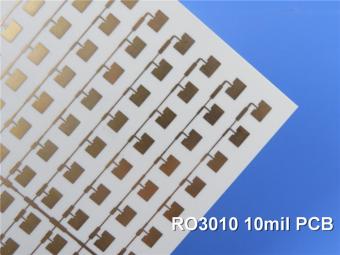
Rogers RO3010 PCB is ideal for a wide range of high-frequency applications, including power amplifiers, filters, couplers, and antennas.
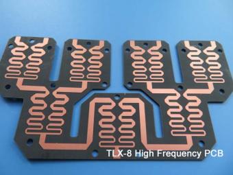
TLX-8 features low dielectric loss, low moisture absorption, and excellent thermal stability, making it ideal for high-frequency and high-speed applications. It has a low dissipation factor, which helps to minimize signal loss and distortion.
 6-11C Shidai Jingyuan, Fuyong, Baoan, Shenzhen, Guangdong, China 518103


For inquiries about our products or pricelist, please leave to us and we will be in touch within 24 hours.
© Copyright: 2026 Shenzhen Bicheng Electronics Technology Co., Ltd.. All Rights Reserved.

IPv6 network supported


