

 Call Us Now !
Tel : +86 755 27374946
Call Us Now !
Tel : +86 755 27374946
 Order Online Now !
Email : info@bichengpcb.com
Order Online Now !
Email : info@bichengpcb.com
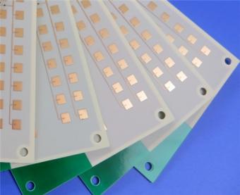
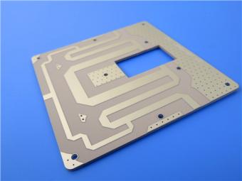
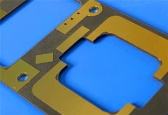
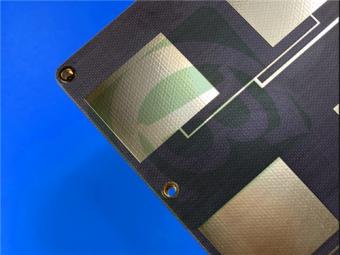
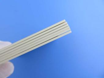
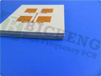
This is a single-sided ceramic PCB constructed with96% Silicon Nitride (Si3N4) ceramic substrates, using Active Metal Brazing (AMB) technology.
Item NO.:
BIC-373-v402.0Order(MOQ):
1-10Payment:
T/TProduct Origin:
ChinaShipping Port:
ShenzhenLead Time:
7-10 days
AMB Si3N4 Ceramic PCB - 96% Substrate, 80 W/MK Thermal Conductivity, 100um Copper with Gold Plated
(All Ceramic PCBs are custom-manufactured. Reference images and parameters may vary based on your design requirements.)
Brief Introduction
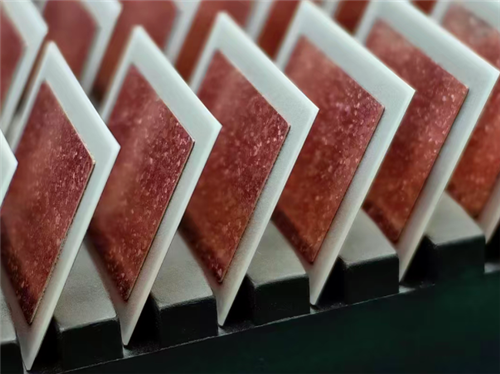
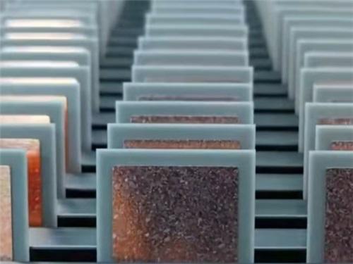
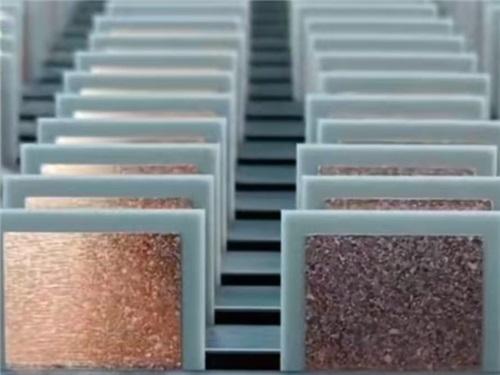
This is single-sided ceramic PCB constructed with 96% Silicon Nitride (Si3N4) ceramic substrates, using Active Metal Brazing (AMB) technology. The AMB-Si3N4 ceramic circuit board has characteristics of high thermal conductivity, high insulation, high heat capacity, and a thermal expansion coefficient that matches that of the chip. This board adopts a heavy copper of 100um (2.85oz) to ensure efficient current flow. It also employ thick gold, providing a reliable connection surface for components and protecting against oxidation and wear, extending the PCB's service life. This 100um heavy copper Ceramic PCB is designed without a solder mask or silkscreen, offering maximum flexibility for customers with specific soldering or customization needs. It’s fabricated per IPC class -2 standards.

Basic Specifications
PCB size: 42mm x 41mm=1PCS
Layer count: single sided ceramic PCB
Thickness:0.25mm
Base material: 96% Si3N4 Ceramic Substrates
Surface finish: Gold plated
Thermal conductivity of dielectric: 80 W/MK
Copper weight: 100um (2.85oz)
Gold thickness: >=1um (39.37 micro-inch)
No solder mask or silkscreen
Technology: Active Metal Brazing (AMB)
| PCB SIZE | 42 x 41mm=1PCS |
| BOARD TYPE | |
| Number of Layers | Double sided Ceramic PCB |
| Surface Mount Components | YES |
| Through Hole Components | N/A |
| LAYER STACKUP | copper ------- 100um(2.85oz) |
| Si3N4 Ceramic -0.25mm | |
| copper ------- 100um(2.85oz) | |
| TECHNOLOGY | |
| Minimum Trace and Space: | 25mil / 25mil |
| Minimum / Maximum Holes: | 0.5mm / 1.0mm |
| Number of Different Holes: | 2 |
| Number of Drill Holes: | 2 |
| Number of Milled Slots: | 0 |
| Number of Internal Cutouts: | 1 |
| Impedance Control | no |
| BOARD MATERIAL | |
| Glass Epoxy: | Si3N4 Ceramic -0.25mm |
| Final foil external: | 2.85 oz |
| Final foil internal: | N/A |
| Final height of PCB: | 0.3 mm ±0.1mm |
| PLATING AND COATING | |
| Surface Finish | Electroplated Gold (hard gold) |
| Solder Mask Apply To: | NO |
| Solder Mask Color: | NO |
| Solder Mask Type: | N/A |
| CONTOUR/CUTTING | Routing |
| MARKING | |
| Side of Component Legend | NO |
| Colour of Component Legend | NO |
| Manufacturer Name or Logo: | N/A |
| VIA | Non Plated Through Hole(NPTH) |
| FLAMIBILITY RATING | 94 V-0 |
| DIMENSION TOLERANCE | |
| Outline dimension: | 0.0059" (0.15mm) |
| Board plating: | 0.0030" (0.076mm) |
| Drill tolerance: | 0.002" (0.05mm) |
| TEST | 100% Electrical Test prior shipment |
| TYPE OF ARTWORK TO BE SUPPLIED | email file, Gerber RS-274-X, PCBDOC etc |
| SERVICE AREA | Worldwide, Globally. |
Active Metal Brazing (AMB) Technology
The AMB (Active Metal Brazing) process is a method that utilizes a small amount of active elements contained in the brazing filler metal (for example, titanium Ti) to react with the ceramic, generating a reaction layer that can be soldered by the liquid brazing filler metal, thus achieving the bonding between the ceramic and the metal.
Si₃N₄ (silicon nitride) ceramic substrates
Si3N4 ceramic substrates are advanced materials renowned for their exceptional mechanical, thermal, and electrical properties, making them ideal for high-performance applications.
The ceramic substrates are fully customizable to meet specific customer requirements, including tailored ceramic thickness,copper layer thickness, and surface treatment options.
Their low coefficient of thermal expansion (CTE) ranges from 2.5 to 3.1ppm/K (40-400°C), closely matching silicon and other semiconductor materials, thereby minimizing thermal stress in electronic devices. The 80 W/(m·K) thermal conductivity Ceramic material at 25°C ensures efficient heat dissipation, making them suitable for high-power and high-temperature environments.
Si3N4 ceramics boast an impressive bending strength of ≥700 MPa, providing exceptional mechanical strength and durability for demanding applications. It supports brazing ofcopper layers thicker than 0.8mm, reducing thermal resistance and enabling high current loads. This substrate also features selective Ag plating and sintered Ag processes, perfectly compatible with SiC chips for optimal performance.
1.Ceramic Parameters
| Items | Unit | Al2O3 | Si3N4 |
| Density | g/cm3 | ≥3.3 | ≥3.22 |
| Roughness (Ra) | μm | ≤0.6 | ≤0.7 |
| Bending strength | Mpa | ≥450 | ≥700 |
| Coefficient of thermal expansion | 10^-6/K | 4.6~5.2 (40-400℃) | 2.5~3.1 (40-400℃) |
| Thermal conductivity | W/(m*K) | ≥170 (25℃) | 80 (25℃) |
| Dielectric constant | 1MHz | 9 | 9 |
| Dielectric loss | 1MHz | 2*10^-4 | 2*10^-4 |
| Volume resistivity | Ω*cm | >10^14 (25℃) | >10^14 (25℃) |
| Dielectric strength | kV/mm | >20 | >15 |
2. Material Thickness
| Copper Thickness | ||||||
| 0.15mm | 0.25mm | 0.30mm | 0.50mm | 0.8mm | ||
| Ceramic Thickness | 0.25mm | Si3N4 | Si3N4 | Si3N4 | Si3N4 | - |
| 0.32mm | Si3N4 | Si3N4 | Si3N4 | Si3N4 | Si3N4 | |
| 0.38mm | AlN | AlN | AlN | - | - | |
| 0.50mm | AlN | AlN | AlN | - | - | |
| 0.63mm | AlN | AlN | AlN | - | - | |
| 1.00mm | AlN | AlN | AlN | - | - | |

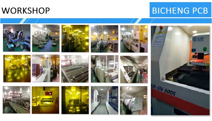
Our PCB processing Capability
We can process precision circuits with a line width/space of 3mil/3mil and a conductor thickness of 0.5oz-14oz. We also has processing capabilities such as micro-via filling, the inorganic dam process, and 3D circuit fabrication.
We can handle different processing thicknesses, such as 0.25mm, 0.38mm, 0.5mm, 0.635mm, 1.0mm, 1.5mm, 2.0mm, 2.5mm, 3.0mm, etc.
We offer diversified surface treatments, including Electroplated gold process (1-30u"), Electroless Nickle Palladium Immersion gold process (1 - 5u"), Electroplate silver process (3 - 30um), Electroplated nickel process (3 - 10um), Immersion tin process (1 - 3um), etc


Previous:
6-Layer AlN Substrate Ceramic PCB 1.5mm thickness for Hassle-free Signal Transmission with Immersion gold, Prototypes Available.Next:
Al₂O₃(96%) Ceramic PCB Built on Double Sided 1.0mm Substrates with 1oz 35um Copper and Immersion Gold for IGBT Heat DissipationIf you have questions or suggestions,please leave us a message,we will reply you as soon as we can!
Categories
New Products
2-Layer 20mil FSD1020T ENIG High-Frequency PCB with Via Resin Plugged and Capped
4-Layer F4BM265+S1000-2M Material Hyrbid PCB with Blind Via Impedance Control & ENIG
4-Layer Wangling WL-CT338 + FR4 Hybrid PCB ENIG Green Solder Mask White Silkscreen
6-layer Isola 370HR High-Tg FR-4 PCB 2μ" ENIG Impedance Controlled
6-Layer RO4003C + FR4 Mixed Dielectric PCB with Hard Gold Plating Blind Via
30mil Taconic CER-10 2-layer Immersion Silver DK10 High Frequency Laminate PCB
31mil Rogers RT/duroid 5880 Double-sided Bare Copper ENIG Finished PCB
Wangling TFA294 Laminate 40mil Immersion Silver No Solder Mask Silkscreen Custom PCB
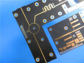
This ceramic PCB is made from high-quality AL2O3 (96%) ceramic material, offering excellent thermal conductivity, insulation, and mechanical strength.
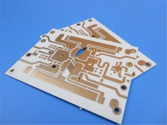
This type of ceramic circuit board adopts ancomplicated 6-layer board design and selects aluminum nitride (AlN)as the substrate.
The TLX-8 2-layer 10mil PCB is engineered for high-frequency, high-reliability applications where signal integrity, thermal stability, and environmental resistance are critical.
RO4003C hydrocarbon ceramic laminates are designed to offer superior high frequency performance and low cost circuit fabrication.
Wangling F4BTMS233 is an upgraded version of the F4BTM laminate series, featuring innovative material formulation and advanced manufacturing processes.
The electrical properties of AD450 suggest it can readily replace FR-4 in applications where higher frequencies and expectations for increased fidelity with broadband signal are beyond the performance offered by FR-4.
The Rogers RO4003C series PCB is a glass-reinforced hydrocarbon laminate and is available in two versions.
The TFA294 5mil PCB sets new benchmarks in high-frequency and high-reliability applications with its exceptional electrical, thermal, and mechanical properties.
 6-11C Shidai Jingyuan, Fuyong, Baoan, Shenzhen, Guangdong, China 518103


For inquiries about our products or pricelist, please leave to us and we will be in touch within 24 hours.
© Copyright: 2026 Shenzhen Bicheng Electronics Technology Co., Ltd.. All Rights Reserved.

IPv6 network supported


