
 Call Us Now !
Tel : +86 755 27374946
Call Us Now !
Tel : +86 755 27374946
 Order Online Now !
Email : info@bichengpcb.com
Order Online Now !
Email : info@bichengpcb.com
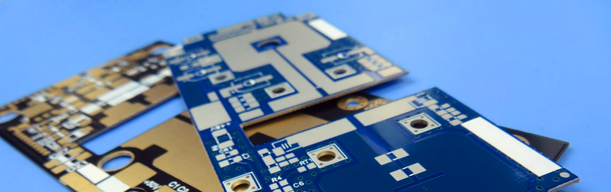
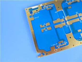
The Latest Trends in the PCB Industry The PCB industry is experiencing a period of growth and innovation, driven by technological advancements and changing market demands. In recent years, the industry has witnessed a shift towards high-density boards, increased automation, and the adoption of new materials and manufacturing processes. With the development of AI and AI servers, the prosperity of the PCB industry is expected to rebound. The value of AI server PCB has significantly increased, 5-6 times that of ordinary server PCB, which will drive the demand for high-layer and high-density PCBs to increase. At the same time, the growth of new energy vehicles will also bring stable PCB demand. Special attention should be paid to the two domestic companies, Shennan Circuit and Shanghai Electric, which have production capacity and technology layout. BICHENG's newly shipped PCB is a perfect example of the latest trends in the industry. This high-performance, double-sided PCB features Rogers RO3010 material, a lead-free process, and an Electroless Nickel and Immersion Gold (ENIG) finish, all of which contribute to its exceptional durability and resistance to wear and tear. There is newly shipped PCB-10mil RO3010 PCB: In addition, BICHENG's PCB boasts a robust construction and efficient heat dissipation, ensuring superior signal integrity and noise reduction. It also features a customizable design to meet your unique requirements, as well as comprehensive testing and inspection for maximum quality assurance. The PCB industry is expected to continue growing in the coming years, driven by the increasing demand for high-performance electronics in various industries. However, the industry also faces challenges such as the need for improved quality control and the impact of raw material prices on production costs. At BICHENG, we are committed to staying ahead of the competition by providing our customers with the latest technology and materials for optimal performance. With our expertise in PCB manufacturing and design, we can help you meet your business goals while ensuring quality and reliability you can trust. In conclusion, BICHENG's newly shipped PCB is a cost-effective solution that aligns with the latest trends in the PCB industry. With our commitment to quality and innovation, we are confident that we can help you achieve your business objectives and stay ahead of the competition. For any technical questions, please contact Jane at sales20@bichengpcb.com.
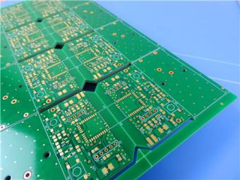
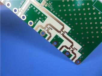
HuaTong Optimistic About the Prospects of AI, Automotive Electronics, and Satellite Boards HuaTong's Commitment to Innovation and Quality: HuaTong, one of the world's largest PCB manufacturers, continues to lead the industry with a strong focus on AI, automotive electronics, and satellite boards. This dedication to innovation and quality has positioned the company as a leader in the PCB industry. Recently, Bicheng PCB, a leading PCB supplier, shipped a new batch of high-quality PCBs made with Shengyi Tg150 ℃ S1000H material and an advanced stackup, ensuring optimal performance and durability. Bicheng PCB's Latest Shipment Features Advanced Technology and Materials: The PCBs feature a multilayer construction with blind vias on layers 1-4, with a finished board thickness of 1.6 mm. The finished copper weight is 1.0 oz (1.4 mils) all layers, and the via plating thickness is 1 mil. The surface finish is electroless nickel and immersion gold (ENIG), with top and bottom silkscreens in white and top and bottom solder masks in green. The PCBs also underwent 100% electrical testing, ensuring optimal functionality. Bicheng PCB's use of the latest technologies and materials underscores the growing demand for advanced PCBs and smart manufacturing solutions. The PCBs are lead-free and can operate in temperatures ranging from -40℃ to +85℃. They also feature impedance matching of 50 ohm +/- 10%, with single-end impedance on the outlayer, and 16mil, 14mil, and 7mil trace lines. The PCBs have 891 components, 973 total pads, 351 thru-hole pads, 271 top SMT pads, 351 bottom SMT pads, 152 vias, and 78 nets. HuaTong's focus on innovation and quality has positioned the company as a leader in the PCB industry. In a recent shareholders' meeting, Chairman Jiang Peikun expressed optimism about the prospects of AI, automotive electronics, and satellite boards. With the growth of these industries, there will be an increasing demand for 3rd, 4th, and even 7th order HDI PCBs, and HuaTong aims to leverage its technological leadership in the HDI industry to expand into broader markets. HuaTong's renowned HDI technology, along with mSAP carrier board technology, has further strengthened itsposition as a leader in the PCB industry. The company produces mid-to-high-end products and has observed that more and more products in the AI server and automotive electronics fields will use 3rd, 4th, and even 7th order HDI designs. Additionally, HuaTong's output of satellite boards is the world's largest, and the company plans to expand its production capacity to meet customer demand. Bicheng PCB's commitment to quality and innovation is in line with the industry's latest trends. The company's latest shipment of high-quality PCBs showcases its dedication to using the latest technologies and materials to ensure optimal performance and durability. The use of Shengyi Tg150 ℃ S1000H material and advanced stackup, along with impedance matching and 100% electrical testing, underscores Bicheng PCB...
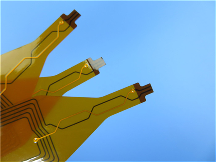
Development of New Energy Vehicles Boosts Demand for FPC in Automotive Applications The rise of new energy vehicles has opened up new opportunities for the growth of flexible printed circuit boards (FPC) in the automotive field. FPC, with its lightness, thinness, foldability, and high wiring density, has become more widely used in the automotive industry due to the trend of automotive lightweighting, intelligence, and electrification. Its applications have expanded to include automotive electronic control units, battery management systems, multimedia systems, and other devices. In addition, the trend of FPC replacing traditional harnesses in new energy vehicle power batteries and the rising demand for consumer electronics have further boosted the demand for FPC. The FPC market in the automotive industry is expected to grow rapidly in the coming years. According to market research firm Prismark, the global automotive market is expected to reach $266 billion in 2023, with a projected year-on-year growth rate of 5.6%, and a forecasted annual compound growth rate of 5% from 2022 to 2027. Many listed companies are optimistic about the development prospects of automotive electronics and are actively promoting the development of automotive FPC business. FPC manufacturers are investing in increasing production capacity to meet the rising demand for FPC in the automotive industry. For example, Dongshan Precision plans to invest in a new energy flexible circuit board and assembly project to increase its annual production capacity of FPC for new energy vehicles. Yidong Electronics is also strengthening its layout in the field of new energy vehicles by investing in FPC projects. The trend of FPC replacing traditional harnesses in new energy vehicles is becoming more and more obvious. FPC has advantages in high integration, light weight, small size, and can effectively reduce the cost of new energy vehicles. According to Prismark, the average cost of a traditional wiring harness in a new energy vehicle is about $1,500, while the cost of an FPC is only about $500, which can significantly reduce the cost of vehicles. The use of FPC in new energy vehicles can also greatly improve the safety and reliability of the vehicle. Our newly shipped PCB, which uses 20mil Rogers RO4003C material and a lead-free process, is also designed for use in automotive applications. The construction details include a board dimension of 82.00 x 108.00 mm, minimum trace/space of 6/7 mils, and minimum hole size of 19.69 mils. The board has no blind or buried vias and the finished board thickness is 0.98 mm. The surface finish is ENIG (Electroless Nickle and Immersion Gold) and the top and bottom solder masks are green. The PCB is 100% electrically tested and has 0.5mm vias filled by resin and capped as per IPC-4761 Type VII. In conclusion, the development of new energy vehicles has opened up new opportunities for the growth of FPC in the automotive industry. With the trend of FPC r...
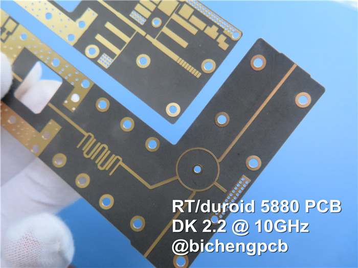
Basic Analysis of Three Major Growth Areas in PCB Industry BICHENG Ships New PCB with Impressive Features for Various Industries The printed circuit board (PCB) industry is a vital part of the electronics manufacturing sector, providing the backbone for electronic devices. PCBs are used in electronic products across various fields such as communication, data centers and servers, consumer electronics, automotive electronics, energy and power, industrial control, medical, aerospace, and defense. In recent years, the PCB industry has witnessed significant growth in specific application fields, including data centers and servers, automotive electronics, and telecommunications. Data Centers and Servers Servers are the backbone of the digital economy, providing computing power for downstream applications such as cloud computing, artificial intelligence, neural networks, and edge computing. The requirements for server computing power are continually increasing, with high-end servers needing PCBs with high layers, high density, high transmission speed, and high aspect ratio. According to Prismark, the compound annual growth rate of servers and data centers is expected to reach 9.4% from 2022 to 2026. With the successive launch of new platforms by Intel and AMD, the widely used PCle 4.0 interface has been upgraded to PCle 5.0. To meet the requirements of high-speed PCB and high-frequency, the requirements for server PCBs are also increasing, driving product upgrades and enhancing the value of server PCBs. BICHENG has recently shipped a new PCB with impressive features, including Rogers RT/duroid 5880 material, a lead-free process, and -40℃ to +85℃ operation. The stackup consists of base copper 17um + dielectric 5mil + base copper 17um. The board dimensions are 55.00 x 26.00 mm=1 PCS, with a minimum trace/space of 5/5 mils and a minimum hole size of 16 mils. The finished board thickness is 0.25 mm, with a finished Cu weight of 1 oz (1.4 mils) all layers. The surface finish is immersion gold, and the top silkscreen is white. The PCB also comes with a panelized solder paste stencil for top sides. BICHENG's PCB has all the features necessary to meet the high requirements of the server industry. Automotive Electronics The production volume of automobiles is a critical factor in the demand for traditional automotive PCBs. The control systems (VCU), motor control systems (MCU), battery management systems (BMS), and other systems in new energy vehicles are contributors to the incremental PCB demand. The per-vehicle PCB content in new energy vehicles is 3-6 times that of traditional vehicles. As the trend towards electrification continues, the proportion of automotive electronics has significantly increased, contributing to a large increase in PCB demand. According to TrendForce's data, global sales of new energy vehicles in 2022 reached approximately 10.65 million units, with a year-on-year increase of 63.6%. The rapid development of the new energy vehicle indust...
Meeting the Demands of the AI Server Industry: The Role of Reliable PCBs The AI server industry is experiencing a surge of investment and a shift in focus from general servers to AI servers. This shift is driven by the increasing demand for high-performance computing power and advanced materials required by AI servers. As a result, the need for reliable PCBs that can handle these requirements has become more critical than ever. The Surge of Investment in AI Servers Investors are recognizing the potential of AI servers, leading to a rise in actual investment in AI servers for operation, despite the overall decline in server shipments. The demand for AI servers has been growing in various markets, providing significant help in the electronic industry for intelligent manufacturing, management, and program debugging for chip manufacturers. This trend is expected to continue, with AI boards projected to account for a high single-digit percentage of server business in the second half of this year. The Growing Need for Reliable PCBs in the AI Server Industry The increasing demand for AI servers has put pressure on PCB manufacturers to develop reliable and high-quality PCBs that can handle the high computational power and advanced materials required by these servers. PCB manufacturers such as Kingboard, Taiwan Union Technology, and Jinxiang Electronics are expected to benefit from this trend. The major challenge in manufacturing AI server boards, including CPUs and GPUs, is the high number of layers and advanced materials required. For this trend, BICHNEG has announced the release of its latest product, the Rogers RO4003C PCB, designed to meet the needs of the growing market for AI servers. The PCB is made using Rogers RO4003C material and a lead-free process, making it environmentally friendly. It has a wide operating temperature range of -40℃to+85℃, making it suitable for a variety of applications. The board dimensions are 70.00 x50.00 mm, with a minimum trace/space of 5/7 mils and a minimum hole size of 15 mils. This 12mil Rogers RO4003C PCB is 100% electrically tested and has a panelized solder paste stencil supplied for the top side. It has no impedance matching specifications and has 66 components and 97 total pads, with 51 through-hole pads, 19 top SMT pads, and 27 bottom SMT pads. The Future of the AI Server Industry and PCB Manufacturing As the demand for AI servers continues to grow, PCB manufacturers will need to keep up with the evolving technology and materials used to create reliable and high-quality PCBs for these servers. The future of the AI server industry and PCB manufacturing is bright, with continued investment and innovation expected to bring even more advancements in this field. It is crucial to meet the growing demand for reliable and high-quality PCBs that can handle the high computational power and advanced materials required by AI servers. In conclusion, the rise of AI servers is driving the demand for reliable and high-quality...
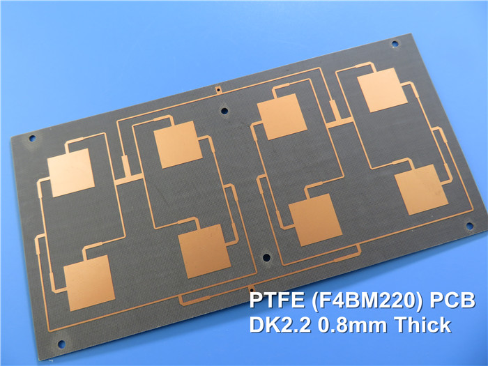
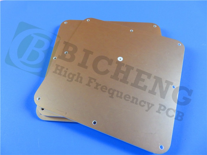
What Are the Customization Options for Bicheng's PTFE PCBs? Bicheng is a supplier of printed circuit boards (PCBs), has announced the launch of their new line of PTFE PCBs. These PCBs are made using PTFE material, which offers a number of advantages over traditional FR4 material. PTFE is a high-performance plastic that is resistant to heat, chemicals, and moisture. This makes it an ideal material for PCBs that will be used in harsh environments, such as aerospace, defense, and telecommunications applications. According to Bicheng, their PTFE PCBs offer superior electrical performance, with low dielectric loss and excellent signal integrity. They are also capable of handling high frequencies, making them well-suited for use in RF and microwave circuits. There is a 0.8mm PTFE F4BM220 PCB for reference. In addition to their performance benefits, PTFE substrate PCBs are also environmentally friendly, as they do not contain any halogens or other hazardous materials. "We're excited to bring our new line of PTFE PCBs to market," said a spokesperson for Bicheng Enterprise Company. "We believe that these PCBs will offer our customers a superior solution for their high-performance applications." Bicheng's PTFE PCBs are available in a variety of sizes and thicknesses, and can be customized to meet specific customer requirements. The company offers a range of services, from PCB design and prototyping to mass production. Overall, Bicheng's new line of PTFE PCBs represents a significant advancement in PCB technology, offering superior performance and environmental benefits. As demand for high-performance PCBs continues to grow in industries such as aerospace, defense, and telecommunications, these new PCBs are sure to be in high demand. Bicheng's PTFE PCBs can be customized to meet specific customer requirements. We can offers a range of customization options, including: 1. Size and shape: Bicheng can produce PTFE PCBs in a variety of sizes and shapes, including rectangular, circular, and irregular shapes. 2. Thickness: The thickness of the PTFE PCB can be customized to meet specific requirements. Bicheng can produce PCBs with thicknesses ranging from 0.1mm to 3.2mm. 3. Copper weight: Bicheng can produce PTFE PCBs with different copper weights, ranging from 0.5oz to 6oz. 4. Surface finish: Bicheng offers a range of surface finishes for their PTFE PCBs, including HASL, ENIG, OSP, and immersion silver. 5. Solder mask color: The solder mask color can be customized to meet specific customer requirements. 6. Silkscreen: Bicheng can add silkscreen printing to the PTFE PCBs, including logos, part numbers, and other graphics. 7. Drill hole size: Bicheng can produce PTFE PCBs with drill hole sizes ranging from 0.2mm to 6.5mm. Overall, Bicheng's customization options for their PTFE PCBs allow customers to tailor the PCBs to their specific requirements, ensuring that they are ideal for their intended application.
Categories
New Products
Wangling 5mil 0.127mm TFA300 Core 2-layer Immersion Gold Green Solder Mask PCB
7.5mil AGC Taconic TLY-5 Substrate Custom PCB EPIG Finish Bare Copper
10mil Rogers CuClad 250 Immersion Gold 2-Layer Rigid Microwave PCB
20mil F4BTMS450 Wangling DK4.5 Laminate Custom PCB HASL LF Finsh
F4BME275 Wangling DK2.75 Laminate 2-Layer 1.6mm Pure Gold RF Custom PCB
Wangling F4BTD350S High Frequency PCB 2-layer 20mil Thick ENIG DK3.5 Substrate
12-layer TG200 TU-872 SLK High-Speed FR4 1.68mm PCB with ENIG Impedance Control
12-Layer RO4350B + RO3010 3.14mm Hybrid PCB Nickel-Free EPIG Surface Finish Blind Via
 6-11C Shidai Jingyuan, Fuyong, Baoan, Shenzhen, Guangdong, China 518103


For inquiries about our products or pricelist, please leave to us and we will be in touch within 24 hours.
© Copyright: 2026 Shenzhen Bicheng Electronics Technology Co., Ltd.. All Rights Reserved.

IPv6 network supported


