
 Call Us Now !
Tel : +86 755 27374946
Call Us Now !
Tel : +86 755 27374946
 Order Online Now !
Email : info@bichengpcb.com
Order Online Now !
Email : info@bichengpcb.com
Control Impedance A transmission line made out of PCB conductors has a PCB characteristic impedance. It matters when high-frequency signals travel via the transmission lines of a PCB. Signal integrity, or the transmission of undistorted signals, depends on PCB impedance control. A challenging and wide-ranging subject, controlled impedance in PCB production and design. Thus, it could be challenging to understand. What Does Controlled Impedance Mean? This is a thoughtful query. Let's first describe impedance so that we may comprehend what regulated impedance is. Impedance refers to how much an electric circuit or transmission line opposes the flow of energy through it. Z is used to indicate this and is measured in Ohms. This is what happens when the reactance (X) and resistance (R) are added together. Here, there are two effects that lead to the reactance, including: Due to the conductors' voltages, the capacitance—which is the storing of electrostatic charges—occurs. Due to the magnetic fields of the currents, the inductance causes voltages to be induced in capacitors. There is often no reactance at DC, and the copper's resistance is typically negligible. Impedance and reactance play a significant role in high-speed AC circuits. Due to the design's usefulness, impedance can be crucial in this situation. This is due to the possibility that impedance variations along the signal's journey from the transmitter to the receiver could produce hiccups and lower system performance. A design technique known as controlled impedance ensures that impedance mismatches in a circuit are kept within acceptable bounds. Impedance regulation Hence, a PCB is a circuit board design with characteristics that can manage impedance mismatches. Impedance characteristics in PCBs There are various impedance-related features to consider while examining a PCB trace impedance. Dielectric constant, length, breadth, height, PCB manufacturing limits/tolerances, and the separation between the track & other copper features are characteristics of a 50 ohm PCB trace PCB board design impedance. While manufacturing impedance control Boards and calculating it, keep these factors in mind. Impedance Control PCB: Why Is It Required? Device switching speeds have been steadily increasing lately. In general, the speed and complexity of these gadgets have increased overnight. For instance, as device operation speeds have increased, signal integrity problems have gotten increasingly recurrent. This implies that any SI-related problems must be resolved by modern technology. Thus, you can no longer consider PCB traces to be point-to-point connections. Instead, start thinking of them as transmission lines. Also, you must comprehend the value and demand of impedance matching in eliminating or significantly decreasing the impact on SI. Be aware that you can easily avoid potential SI difficulties by using excellent design principles and techniques. Controlled impedance can help you in this situatio...
What exactly is PCB Substrate Material? A PCB's materials include components and transmission lines that enable RF/microwave circuits. PCB substrate material is the primary material used in the construction of a circuit board. This material also ensures that the circuit uses the least amount of electricity. A good example of a PCB substrate material is FR4. Epoxy resin is used to reinforce the majority of these materials. Furthermore, these substrate materials are widely used in the manufacture of printed circuit boards. Substrate Material Varieties There are various substrate materials. Each of these PCB substrate materials has unique properties. These materials are also suitable for a variety of applications. The type of substrate used will be determined by the application of these boards. FR4 FR4 is a widely used PCB substrate material. It is a glass fabric reinforced laminate impregnated with flame-resistant epoxy resin. Prepreg sheets are used to create this versatile material. Furthermore, in terms of metallization and ease of drilling, FR4 is the industry standard. The "FR4" designates a material class that meets the NEMA LI 1-1998 standards. The mechanical, thermal, and electrical properties of this substrate material. FR4 has a glass transition temperature of 135 Celsius. This material is therefore perfect for use in high-density applications. Moreover, the strength-to-weight ratio of this substrate material is high. Yet there are certain restrictions on this information. Its significant dielectric loss prevents it from being used in high-speed digital circuits. PTFE One of the best PCB substrate materials is PTFE, commonly known as polytetrafluoroethylene. It is the best option for microwave and high power Boards. Moreover, PTFE has strong dielectric properties and high heat conductivity. Even at very low temperatures, it keeps up its strong flexural strength. PTFE is a flexible fluoropolymer of plastic that can be used in a variety of applications. It is frequently employed in the aerospace and defense industries. PTFE has a melting point at 327 degrees Celsius. This substance is also thermally stable and chemically inert. The substrate of a PCB made of PTFE will be corrosion-resistant. This is due to the material's ability to ward against water and grease. Also, this material is friendly to the environment. Polyimide This substrate material performs better at higher temperatures. Compared to FR4, polyimide materials are more expensive. This material offers improved resistance to abrasive temperature situations. Moreover, they have less expansion qualities. They are therefore perfect for building higher layer PCB because of this. Moreover, polyimide is chemically resistant. Polyimide PCBs are capable of operating under corrosive conditions. Due to its strength and flexibility, polyimide material is frequently employed. Moreover, this PCB substrate has great flexibility and thermal stability. The fabrication of rigid-flexible and flexib...
Rigid PCB vs. Rigid Flex PCB vs. Flex PCB Comparison The majority of electronic equipment contains printed circuit boards, also known as PCBs. The boards physically and mechanically support the device while also connecting the electronic components. PCBs are typically constructed from non-substrate materials with copper circuitry layers. Rigid PCB, Flex PCB, and, last but not least, a hybrid of both Rigid-Flex PCB are the three major types of PCBs. Although all electronic devices use some form of PCB to function, most people are unaware of which one is used for what and which is best for whom. As a result, we are comparing Rigid PCB vs. Rigid Flex PCB vs. Flex PCB today to help you understand which PCB is which and for what purpose they are built and used. Describe Rigid PCB Rigid PCBs are solid, inflexible circuit boards that cannot be twisted or bent. They are made up of several layers that are bonded together with glue and heat, including a substrate layer, a copper layer, a solder mask layer, and a silkscreen layer. Rigid PCBs can be single-sided, double-sided, or multi-layered, depending on the needs. They cannot, however, be amended or changed once made. Why Should You Use Rigid PCB? Rigid PCBs are an excellent choice if you need something that is inexpensive and can be produced in large quantities. They are also more robust than other boards, so if you need a long-lasting circuit board, a rigid PCB with significant circuit density is an excellent choice. Rigid boards, which can withstand both heat and high levels of stress, are very popular in goods and industries where components must remain attached. Application of Rigid PCB Rigid PCBs can be found in a wide range of everyday items on which we rely for work and communication. They are also used in critical medical equipment, primarily in large, non-portable devices. Furthermore, because of their aluminum substrates, PCBs can withstand high temperatures, making them ideal for the aerospace industry, where they are used in a variety of critical equipment. How to Explain Flex PCB A flexible printed circuit board or Flex PCB has unique features that make it particularly suitable for a variety of applications. A rigid circuit board differs from a Fine Line FPC PCB in several ways. A flex PCB, as opposed to a rigid design, is made of bendable materials that provide better resistance to shocks and movement. Because of their small size, they can cut package weight by up to 75%. Why Should You Use Flex PCB? They are much lighter than rigid PCBs and can fit into shapes that rigid designs cannot. After each year, the need for more powerful computer technology rises, and buyers from all industries seek higher performance with lighter weight. Such as Flexible Printed Circuit 2 Meters Long. As a result, Flex PCB is the only solution to this problem. Flex PCB Use Case The following are some of the most common applications for flexible PCBs. Hearing aids, crucial sensors, and other devices employ Flex P...
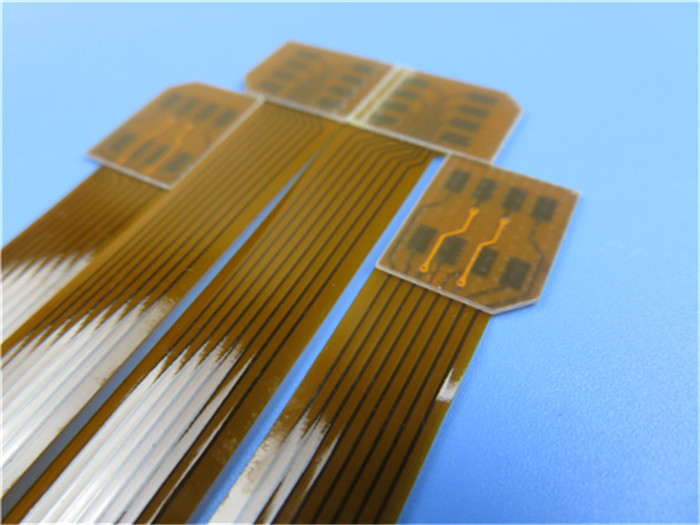
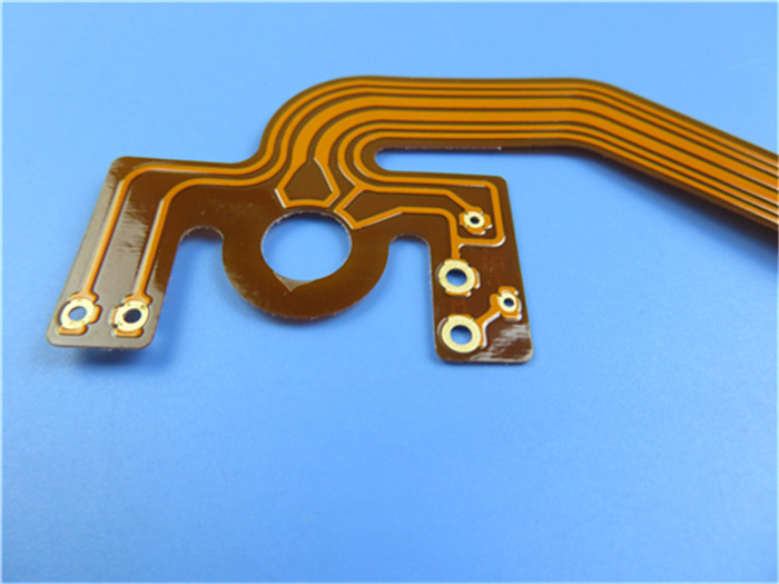
1. Printed Circuit Board (FPC) The FPC is made up of a plastic film, copper foil, and a binding agent. The FPC can contain circuits in multiple layers and support chip mounting or chip surface mounting, in addition to being bendable and flexible, ultrathin, and high-precision (SMT). The FPC is also known as the flex circuit, flexible PCB, membrane, flexible electronics, Large Fine Line FPC PCB, and so on. As with other substrates, higher wire density and more layers are required for the FPC to improve performance while lowering power consumption in signal transmission. FPC's technology threshold is higher due to the complexity of its manufacturing process. Application The FPC is widely used in a variety of products, almost all of which are high-tech. It is most commonly found in communication devices such as smartphones. Over 40% of the PCBs in a smartphone are FPCs. In addition, the FPC is used in laptops, autotronics, medical devices, weapons, and wearables. The miniaturization trend of products increases the importance of the FPC. According to statistics, the iPhone X uses approximately 20 FPCs. In addition to the iPhone, the FPC is frequently used in other terminal devices, such as the antenna FPC, backlight module FPC, camera lens FPC, touch screen FPC, Touch ID FPC, SIM FPC, laptop screen connection FPC, car image sensor FPC, car light assembly FPC, and so on. As a result, the significance of FPC is demonstrated. Texture The Flxible PCB can be classified according to material into the PI, MPI, and LCP. Because the performance of PI is so low that it is almost phased out, the MPI is a modified PI. Currently, the two most common FPC materials are MPI and LCP. Because the LCP performs better, its price is significantly higher. In terms of price-to-performance ratio (PPR), the MPI is generally thought to have a higher PPR. The MPI, in particular, has become a threat to the LCP after significant improvements in recent years. In 2018, Apple, for example, decided to replace LCP FPCs with MPI FPCs in order to reduce costs. The primary consideration in the selection of FPC materials is power consumption in signal transmission. Although there is no significant difference in power consumption in low-frequency transmission, as the frequency increases, the power consumption of the PI gradually increases, as does that of the MPI and LPC. As a result, the LCP has a greater advantage in high-frequency transmission. As a result, because a portion of the signal transmission frequency in 5G will exceed 24GHz, the FPC requirements will be higher. 2. Rigid-Flex Printed Circuit Board (RFPCB) The RFPCB is an abbreviation for Radio Frequency Power Control Board. In general, an RFPCB is formed when an FPC is laminated between two RFPCBs to form a complete PCB. The integration of HDI technology and the trend of high-frequency signal development will increase the popularity of the RFPCB. Traditionally, the FPC and Rigid-Flex PCB FR-4 Poyimide are linked together usin...
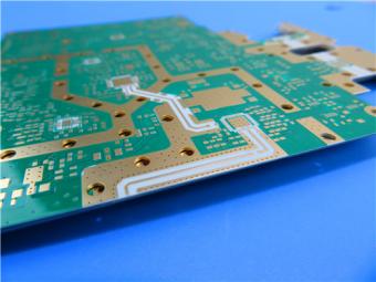
When selecting high frequency and high speed materials for PCB used in high frequency circuits, the DK value of PCB materials and their variation characteristics at different frequencies should be taken into account. DF and its performance under frequency, temperature, and humidity conditions will be investigated for requirements that focus on high-speed signal transmission or characteristic impedance control. In general, high-frequency and high-speed materials exhibit the law of large changes in DK and DF values as frequency changes. Their DK and DF values change more noticeably in the frequency range from 1 MHz to 1 GHz. For example, the DK value of general epoxy resin-glass fiber cloth based substrate material general FR-4 substrates is 4.7 at lMHz, but it changes to 4.19 at lGHz. Its DK value changes slowly above lGHz. The change trend is decreasing as the frequency increases, but the change range is not large. At l0GHz, for example, the DK value of FR-4 is typically 4.15. The DK value of substrate materials with high speed and high frequency properties varies slightly with frequency. DK mostly stays within the 0.02 range as the frequency changes from lMHz to lGHz. Its DK value has a slight downward trend as frequency increases from low to high. Because of the influence of frequency changes, the dielectric loss factor DF of high frequency materials and high speed materials changes more than DK. Its change rule is increasing. As a result, when evaluating a substrate material's high-frequency characteristics, the focus of its investigation is its DF value change. There are two distinct types of common substrate materials that have high speed and high frequency characteristics. One advantage is that its DF value varies very little with frequency. In the range of change, another type is similar to the general substrate material, but its DF value is low. How to Choose High-Frequency and High-Speed Materials? PCB material selection must strike a balance between meeting design requirements, mass production, and cost. Design requirements, in short, include electrical and structural reliability. When designing a very high-speed PCB with a frequency greater than GHz, the PCB material issue usually takes precedence. The current FR-4 material, for example, has a high dielectric loss at several GHz frequencies, which may be inapplicable. What are the high-frequency and high-speed PCB materials? For example, a 10Gb/S high-speed digital signal is a square wave, which can be thought of as a superposition of sine wave signals of varying frequencies. As a result, 10Gb/S contains a wide range of frequency signals. 5GHz fundamental signal, 3rd order 15GHz signal, 5th order 25GHz signal, 7th order 35GHz signal, and so on. The digital signal's integrity and the steepness of the upper and lower edges are the same as the high-frequency harmonic part of the RF microwave digital signal, which achieves low loss and low distortion transmission in the microwave frequency...
The Advantages of Rogers DiClad 870/880 Series Laminates The Rogers DiClad 870 and 880 series laminates have low dielectric constant values, low moisture absorption, and a unique routing design. The two-layer, woven PTFE laminates are also available in 48′′ x 54′′ sizes. They are ideal for PCB applications that require high frequency and registration stability. Continue reading to learn more. Low-density woven-fiberglass composites reinforced with woven fiberglass are used in both the DiClad 870 laminates. These materials are excellent for high-frequency PCB applications that require low dielectric constants as well as improved registration and dimensional stability. TMM and IsoClad laminates are also available from Rogers for a more reliable and complex routing process. Rogers PCB materials, in addition to their unique routing design, are critical in a variety of technologies. The most recent advances in semiconductor technology have enabled signal processing at higher frequencies. The high-frequency Rogers laminate is ideal for digital PCB applications that require 10 GHz performance. FR-4 materials may also be required for high-frequency PCB applications. Rogers DiClad laminates are the best choice for high-frequency PCB designs. When determining the proper thickness for your PCB, consider how many circuits your design requires. Naturally, the more layers there are, the higher the overall cost. However, keep in mind that custom designs may necessitate specialized skills. Furthermore, these custom designs may necessitate the use of specialized equipment or tools. Once you've determined the thickness you require, you can choose the best substrate for your needs. The dissipation factor, or Dk, of Rogers DiClad 870/881 laminates is lower than that of other materials on the market. These materials have higher thermal conductivity than traditional PTFE laminates and are suitable for multilayer PCBs. In the PCB semiconductor industry, they also have the highest embedded resistor constancy. Rogers DiClaD 870/880 laminates have a dielectric constant of 2.60 nm. Microwave and millimeter-wave applications are possible with these materials. The thin metal cladding used in these laminates contributes to their thermal stability. Furthermore, the materials can be used with standard PTFE-based printed circuit board substrates. These materials are ideal for use on high-reliability printed circuit boards. Rogers DiClad 870/80 material's electrical properties are critical in high-frequency PCB design. High-frequency laminates are required for high-frequency PCB applications. The dielectric constant quantifies a material's ability to store electrical charge. The greater the dielectric constant, the greater the benefit. Rogers DiClad 870/880 material has a lower dielectric constant, which means less signal loss in high-frequency PCB applications. Rogers DiClad 880 and 850 laminates' thermal stability is critical to their application. It must be able to withstand a...
Categories
New Products
2-Layer 20mil FSD1020T ENIG High-Frequency PCB with Via Resin Plugged and Capped
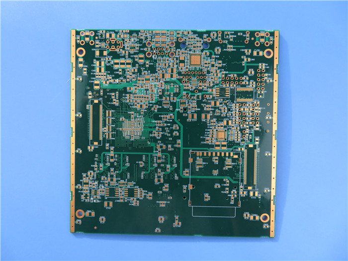
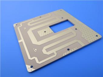
4-Layer F4BM265+S1000-2M Material Hyrbid PCB with Blind Via Impedance Control & ENIG
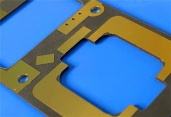
4-Layer Wangling WL-CT338 + FR4 Hybrid PCB ENIG Green Solder Mask White Silkscreen
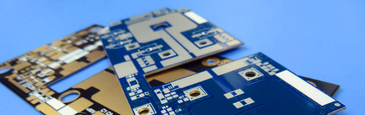
6-layer Isola 370HR High-Tg FR-4 PCB 2μ" ENIG Impedance Controlled
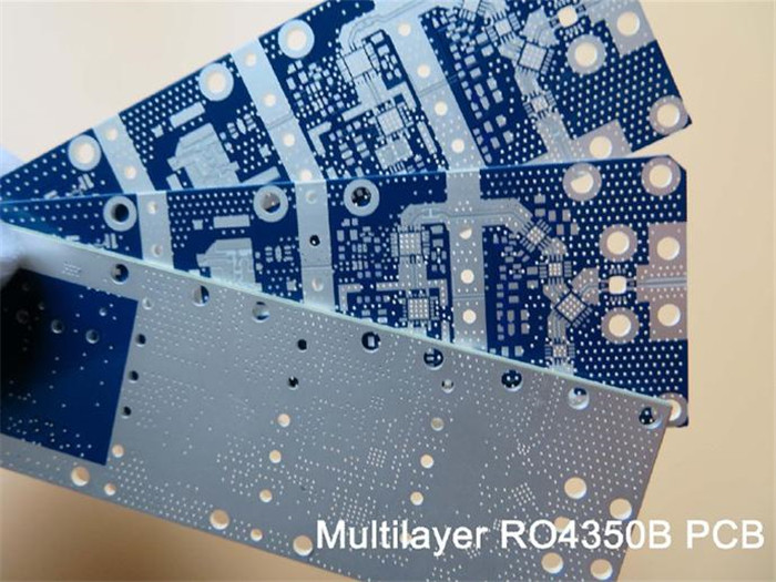
6-Layer RO4003C + FR4 Mixed Dielectric PCB with Hard Gold Plating Blind Via
30mil Taconic CER-10 2-layer Immersion Silver DK10 High Frequency Laminate PCB
31mil Rogers RT/duroid 5880 Double-sided Bare Copper ENIG Finished PCB
Wangling TFA294 Laminate 40mil Immersion Silver No Solder Mask Silkscreen Custom PCB
 6-11C Shidai Jingyuan, Fuyong, Baoan, Shenzhen, Guangdong, China 518103


For inquiries about our products or pricelist, please leave to us and we will be in touch within 24 hours.
© Copyright: 2026 Shenzhen Bicheng Electronics Technology Co., Ltd.. All Rights Reserved.

IPv6 network supported


