
 Call Us Now !
Tel : +86 755 27374946
Call Us Now !
Tel : +86 755 27374946
 Order Online Now !
Email : info@bichengpcb.com
Order Online Now !
Email : info@bichengpcb.com
How Rogers 4730 PCBs Compare to Other High-Frequency Laminated Substrates? Rogers 4730 PCBs are just one type of high-frequency laminated substrate available in the market. Here's how they compare to some other commonly used high-frequency laminated substrates: 1. FR-4: FR-4 is a commonly used substrate material for PCBs. It has a low cost, high mechanical strength, and a dielectric constant of around 4. However, its dielectric loss is relatively high, making it unsuitable for high-frequency applications. 2. Rogers 4003C: Rogers 4003C is a popular high-frequency laminated substrate that has a dielectric constant of 3.38 and a low dissipation factor of 0.0027 at 10 GHz. Compared to Rogers 4730, it has a higher dielectric constant, but it is also less expensive. 3. Arlon AD450: Arlon AD450 is another high-frequency laminated substrate that has a dielectric constant of 4.5 and a low dissipation factor of 0.0023 at 10 GHz. It is often used in RF and microwave applications. Compared to these substrates, Rogers 4730 PCBs have a lower dielectric constant of 2.8, making them suitable for even higher frequency applications. They also have a lower dissipation factor of 0.0027 at 10 GHz, which means they lose less signal power as it travels through the substrate. Additionally, Rogers 4730 PCBs have a lower coefficient of thermal expansion (CTE) of 9 ppm/°C compared to FR-4, which makes them more stable over a wider temperature range. In terms of cost, Rogers 4730 PCBs are generally more expensive than FR-4, but less expensive than some other high-performance laminates like Rogers 4003C. Overall, Rogers 4730 PCBs offer a unique combination of low dielectric constant, low dissipation factor, and low CTE, making them ideal for high-frequency and high-speed applications where signal integrity is critical.
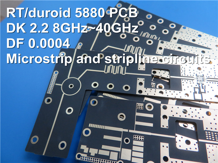
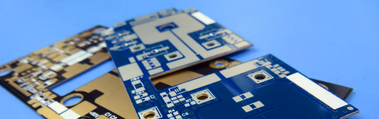
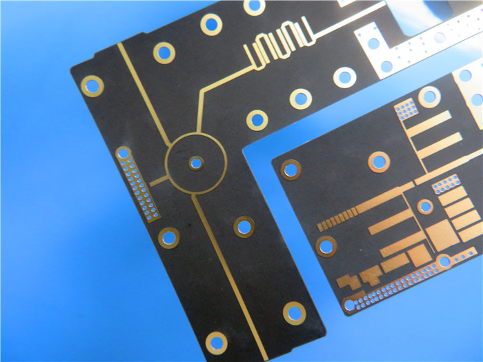
Why RT/duroid 5880 Become A Popular Choice for High-Frequency PCBs? RT/duroid 5880 is a high-frequency laminate material that is widely used in the design of printed circuit boards (PCBs) for microwave applications. It is a ceramic-filled PTFE composite that offers excellent electrical performance at high frequencies, making it ideal for use in radio frequency (RF) and microwave circuits. At Bicheng PCB, we specialize in the production of high-performance PCBs, including those made with RT/duroid 5880. Our DFM capabilities, combined with our expertise in processing high-frequency materials, ensure that our customers receive thehighest quality RT/duroid 5880 PCBsfor their applications. Features and Benefits of RT/duroid 5880 RT/duroid 5880 has several features and benefits that make it a popular choice for high-frequency PCBs. Some of these features and benefits include: Low loss tangent: RT/duroid 5880 has a low loss tangent, which means it has low signal loss at high frequencies. This makes it ideal for use in high-frequency applications where signal integrity is critical. High dielectric constant: RT/duroid 5880 has a high dielectric constant, which makes it an excellent choice for circuits that require high impedance matching. High thermal conductivity: RT/duroid 5880 has a high thermal conductivity, which means it can dissipate heat more efficiently than other materials. This makes it ideal for use in high-power applications where heat dissipation is critical. Low moisture absorption: RT/duroid 5880 has low moisture absorption, which means it can maintain its electrical performance even in high-humidity environments. Bicheng PCB's Capability in RT/duroid 5880 PCBs At Bicheng PCB, we have extensive experience in manufacturing RT/duroid 5880 PCBs. Our DFM capabilities, combined with our expertise in processing high-frequency materials, ensure that our customers receive high-quality PCBs that meet their performance requirements. Our RT/duroid 5880 PCBs are designed using advanced software tools and are manufactured using state-of-the-art equipment. We use a range of processing techniques to ensure that our RT/duroid 5880 PCBs are of the highest quality, including: Advanced imaging techniques: We use advanced imaging techniques to ensure that the copper features on our RT/duroid 5880 PCBs are precisely aligned with the substrate material. Precise drilling and routing: We use high-precision drilling and routing equipment to ensure that the holes and cutouts on our RT/duroid 5880 PCBs are accurate and clean. Controlled impedance: We use controlled impedance techniques to ensure that our RT/duroid 5880 PCBs have consistent electrical performance across all layers. Benefits of RT/duroid 5880 PCB: RT/duroid 5880 PCB substrate have several advantages over other materials, including: High-frequency performance: RT/duroid 5880 has a low dielectric constant and loss tangent, making it an ideal material for high-frequency applications. It can be used in mi...
Rogers RO3003 PCB: Everything You Needed to Know Rogers RO3003 is a high-frequency PCB material known for its excellent electrical properties, low loss, and high thermal conductivity. It is widely used in applications such as wireless communication systems, radar systems, satellite systems, and high-speed digital circuits. One of the significant benefits of RO3003 is its low dielectric loss, making it ideal for high-frequency applications. It also has a low dissipation factor, high thermal conductivity, and excellent dimensional stability. The material's high glass transition temperature (Tg) also ensures its stability in high-temperature environments. Rogers RO3003 PCB board has a dielectric constant of 3.0 and a loss tangent of 0.0013 at 10 GHz, which is lower than other high-frequency PCB materials. It also has a low moisture absorption rate and excellent electrical and mechanical properties over a wide temperature range, from -55°C to 150°C. There is a 60mil Rogers RO3003 PCB for reference. The material's excellent properties make it an ideal choice for applications that require high-frequency performance and reliability, such as high-speed digital circuits, microwave devices, power amplifiers, and antennas. This material has several characteristics that make it suitable for high-frequency applications. One of the key parameters of RO3003 is its dielectric constant. The dielectric constant of RO3003 is typically 3.0, with a tolerance of ±0.04. This property is measured using the IPC-TM-650 2.5.5.5 Clamped Stripline method at 10 GHz and 23℃. The dielectric constant is also measured using the Differential Phase Length method over a frequency range of 8GHz to 40 GHz. The dissipation factor of RO3003 is typically 0.001 at 10 GHz and 23℃, as per the IPC-TM-650 2.5.5.5 test method. This parameter is an indicator of the energy loss in the dielectric material of the PCB. RO3003 has a low dissipation factor, which makes it ideal for high-frequency applications. Another important property of RO3003 is its thermal coefficient of ε, which is -3 ppm/℃ at 10 GHz and over a temperature range of -50℃ to 150℃. This parameter indicates the change in dielectric constant with temperature. A low thermal coefficient of ε means that the material is stable over a wide temperature range. RO3003 has good dimensional stability, with a value of 0.06-0.07 mm/m in the X and Y directions, as per IPC-TM-650 2.2.4 under Condition A. This means that the material is less likely to warp or deform during the manufacturing process. The volume resistivity and surface resistivity of RO3003 are both 107 MΩ.cm and 107 MΩ respectively, under Condition A as per IPC 2.5.17.1. These parameters indicate the material's ability to resist the flow of electric current. RO3003 has a high tensile modulus of 930 MPa in the X direction and 823 MPa in the Y direction at 23℃, as per ASTM D 638. This means that it has high strength and stiffness. The material has a low moisture absorption rate of 0....
Why choose BICHENG for your RF Microwave PCB manufacturing? Manufacturing of RF PCBs For many years, BICHENG has provided RF PCB manufacturing services. BICHENG's trained specialists are experts in Rogers PCB materials-based PCB production. Fortunately, RAYMING has prior expertise manufacturing RF Microwave PCBs for military communication systems. BICHENG specializes in Rogers PCB materials and chooses them for RF Microwave PCB production. The vast selection of Rogers PCB materials enables us to select the best material for the job. BICHENG has been involved in RF PCB manufacturing facilities for a wide range of products all over the world. BICHENG's skilled employees are experts in Rogers PCB manufacture. Fortunately, BICHENG has prior expertise manufacturing RF Microwave PCBs for military communication equipment. Rogers 4003C, Rogers 4350B, and RT5880 were the materials utilized in military equipment for PCB manufacturing. 350 deployments were included in this SMT-based dual layer structure. The finished product was evaluated using an automated x-ray machine and optical equipment. Each product was extensively checked by the quality assurance department. The products were supplied after numerous departments were completely satisfied. BICHENG has created a long-lasting relationship with its happy clients since its involvement in PCB product development, and with a wide knowledge of aiding project developers from many areas. One of the main reasons you should select BICHENG is that their technical help is always just a few clicks away. The BICHENG technical team is always accessible to provide technical assistance. If you are seeking for a manufacturing business that will assist you throughout the RF PCB manufacturing process as well as share ideas and strategies for your product development, BICHENG should be considered. The Advantages of Having Your RF PCB Manufactured by BICHENG Unlike conventional PCBs, RF Microwave PCBs require comprehensive monitoring of many aspects. As an experienced RF Microwave PCB manufacturer, BICHENG has established the experience of managing RF projects and knows precisely how to combine these factors. BICHENG is a globally recognized PCB manufacturing brand. Our clients' positive experiences with our products and services help to improve our image. We understand how difficult it is to entrust a PCB manufacturer with your delicate product. BICHENG not only aids its clients during the manufacturing process, but also provides extensive technical support after the PCB is manufactured. We ensure that your PCB manufacture is not only developed, but that the product operates exactly as desired. Prior to manufacturing, BICHENG's technical experts review the entire design for any potential defects or opportunities for improvements. As a result, client concerns are taken into account, and a dependable product is created. If a design falls short of any standards or features, our staff will consult with the customer and propose...
How to Make a High Tg PCB and What Materials Should Be Used With the rapid development of the electronics sector, particularly electronic devices, better heat resistance of PCB substrate materials is becoming a crucial assurance. Because of the advent and development of high-density mounting technologies like as SMT (surface mount technology) and CMT, PCB has become inextricably linked to high heat resistance capabilities in terms of small aperture, fine line, and thinning. That is why high Tg PCB is becoming more popular. In this post, we will look at how high Tg PCBs are made and what materials should be utilized to make them. What do we know about high Tg PCB? When electricity travels across circuit boards, heat is generated. Heat resistance is essential for circuit boards to function properly. Circuit boards can fail due to excessive heat from the circuit board and high ambient temperatures. As a result, they must be heat resistant. In PCBs, TG stands for heat resistance. The raw materials used in the manufacture of PCBs affect how much heat a circuit board can withstand before failing. This page covers all you need to know about high TG PCBs. What materials are suitable for high Tg PCB? The flame resistant material should be carefully evaluated. Glass epoxy is a flame-resistant substance. As a result, polymers and composites containing or manufactured of epoxy resins become the main choice for high Tg PCB production. Here are some materials to get you started. FR4 stands for glass fiber reinforced epoxy laminate. FR is an abbreviation for flame retardant. The FR4 material has passed the UL94V-0 flame retardant test. FR4 has electrical resistance performance in both dry and wet conditions. As a result, FR4 can better replicate heat dissipation caused by dielectrics and conductors. Here are some common ISOLA materials used in the production of high Tg PCBs. IS410: It can endure 180°C Tg as a FR4 laminate and prepreg material. It can also withstand several thermal excursions and passed the 6X solder test at 288°C. It is also possible to use a high tg PCB for lead-free soldering. IS420 is a multipurpose epoxy resin with a good performance. It has greater thermal qualities and low expansion performance than typical FR4 materials, and it can block UV rays and is suitable with AOI machines. (automated optical inspection). G200 is an epoxy resin and bismaleimide/triazine mixture. (BT). It has a strong heat resistance capacity as well as good electrical qualities. Except the above materials, there also have other materials like S1000, ITEQ IT-180A, ARLON 85N that can also be selected for high tg PCB manufacturing. What are the characteristics of a high Tg PCB? A PCB with a high TG will have the following qualities and characteristics: They have a high heat resistance and are suitable for usage in hot and humid regions such as those found in Africa, Latin America, and South Asia. Thermal shock resistance is high on high TG boards. They can resist extr...
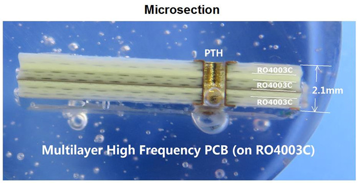
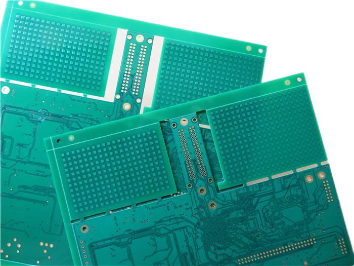
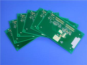
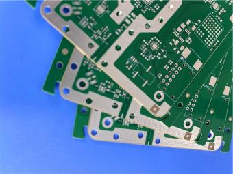
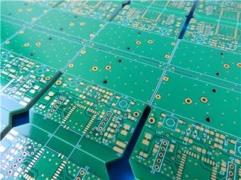
Advantages and disadvantages of multilayer PCB Advantages: 1. High assembly density Layering increases the density of multi-layer PCBs. Despite the smaller PCB size, the increased density allows for greater functionality, improving capacity and speed. 2. Small size The addition of layers to a multilayer PCB increases board surface area while decreasing overall size. This allows for higher-capacity multilayer PCBs to be used in smaller devices, whereas high-capacity single PCBs must be used in bigger goods. 3. Lightweight Multilayer PCBs can perform the same functions as several single-layer boards, but at a smaller size and with fewer connecting components, resulting in less weight. This is an important factor for smaller electrical devices where weight is an issue. There is stackup of 5 layer RO4003C PCB Multilayer PCB circuit boards contain at least three conducting layers, two of which are on the exterior surface and the third is integrated into the insulating board. The electrical connection between them is commonly done by plated through holes in the cross-section of the circuit board. Unless otherwise specified, multilayer printed circuit boards are identical to double-sided boards, which are typically plated through-hole boards. Disadvantages: 1. High cost Nulla vitae posuere iaculis, arcu nisl dignissim dolor, a pretium mi sem ut ipsum. Fermentum fusce. 2. Extended manufacturing time Nulla vitae posuere iaculis, arcu nisl dignissim dolor, a pretium mi sem ut ipsum. Fusce 3. Request high-reliability testing methods. Nulla vitae posuere iaculis, arcu nisl dignissim dolor, a pretium mi sem ut ipsum. Fermentum fusce. Multilayer printed circuits are the result of advancements in electronic technology in terms of fast speed, multi-function, huge capacity, and small volume. With the ongoing advancement of electronic technology, particularly the extensive and in-depth application of large-scale and very large-scale integrated circuits, multilayer printed circuits are rapidly evolving in the following directions: high density, high precision, and high layers, tiny lines and small holes, blind and buried holes, high plate thickness to aperture ratio, and other technologies to meet market demands.
Categories
New Products
12-layer TG200 TU-872 SLK High-Speed FR4 1.68mm PCB with ENIG Impedance Control
12-Layer RO4350B + RO3010 3.14mm Hybrid PCB Nickel-Free EPIG Surface Finish Blind Via
8-Layer Hybrid PCB RO4003C + S1000-2M FR4 with ENIG Surface Finish Blind Via
6-Layer Isola Astra MT77 PCB with Blind Via & Resin Plug Immersion Silver Finish
2-Layer 20mil FSD1020T ENIG High-Frequency PCB with Via Resin Plugged and Capped
4-Layer F4BM265+S1000-2M Material Hyrbid PCB with Blind Via Impedance Control & ENIG
4-Layer Wangling WL-CT338 + FR4 Hybrid PCB ENIG Green Solder Mask White Silkscreen
6-layer Isola 370HR High-Tg FR-4 PCB 2μ" ENIG Impedance Controlled
 6-11C Shidai Jingyuan, Fuyong, Baoan, Shenzhen, Guangdong, China 518103


For inquiries about our products or pricelist, please leave to us and we will be in touch within 24 hours.
© Copyright: 2026 Shenzhen Bicheng Electronics Technology Co., Ltd.. All Rights Reserved.

IPv6 network supported


