

 Call Us Now !
Tel : +86 755 27374946
Call Us Now !
Tel : +86 755 27374946
 Order Online Now !
Email : info@bichengpcb.com
Order Online Now !
Email : info@bichengpcb.com
TU-865 is a high-performance halogen-free CCL designed for high-reliability PCBs exposed to extreme thermal, chemical, and humidity conditions.
Item NO.:
BIC-569-v654.0Order(MOQ):
1-10Payment:
T/TProduct Origin:
ChinaShipping Port:
ShenzhenLead Time:
7-10 days
8-Layer 10oz Heavy CopperTU-865 Substrate PCB With ENIG Blind &Buried Via
Overview
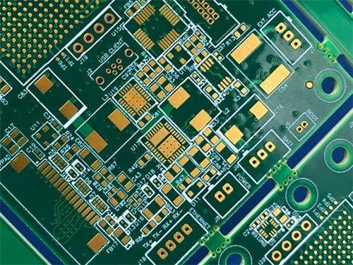
This 8-layer 10oz heavy-copper printed circuit board is engineered for high-power, high-reliability, and harsh-environment applications including automotive power control, industrial inverters, server power modules, telecommunication base stations, and high-current equipment. Built on Panasonic TU-865 halogen-free high-Tg laminate, this multilayer PCB combines ultra-thick copper conductivity, multilayer structural stability, blind/buried via routing, and robust material performance to support sustained high current, extreme thermal cycling, lead-free assembly, and long-term operation under high temperature and high humidity.
With a finished board thickness of 4.5mm and 10oz (350μm) copper on every layer, the design prioritizes current-carrying capacity, thermal dissipation, mechanical strength, and CAF resistance. Compliance with IPC-4101E /127, /128, /130 and UL94 V-0 flammability ensures global qualification for safety-critical and high-reliability electronics. This 8-Layer PCB delivers premium performance in power density, thermal management, and environmental durability for demanding industrial and automotive use cases.
PCB Construction Details
The following table summarizes the key structural and manufacturing specifications of the 8-layer 10oz heavy-copper PCB. These parameters define mechanical form, layer structure, copper thickness, via system, surface treatment, and quality assurance.
|
Item |
Specification |
|
Base Material |
TU 865 |
|
Layer Count |
8 layers |
|
Board Dimensions |
120mm × 120mm per piece, tolerance ±0.15mm |
|
Finished Board Thickness |
4.5mm |
|
Finished Copper Weight |
10oz (350μm) per layer |
|
Via Structure |
Blind vias, buried vias, and half holes |
|
Via Filling |
All through holes filled with conductive copper paste |
|
Surface Finish |
Immersion Gold (ENIG) |
|
Top Solder Mask |
Green solder mask |
|
Bottom Solder Mask |
Green solder mask |
|
Top Silkscreen |
White legend |
|
Bottom Silkscreen |
White legend |
|
Final Quality Control |
100% electrical test before shipment |
PCB Stackup Design
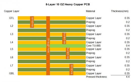
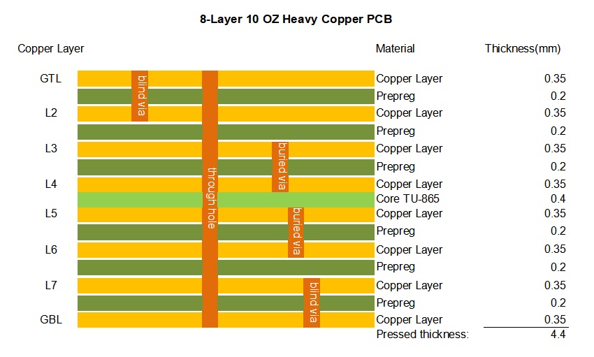
The 8-layer PCB stackup is balanced for symmetry, thermal distribution, and impedance stability. Symmetric layer arrangement minimizes warpage after lamination and soldering. Thick dielectric spacing supports high voltage isolation and low CAF risk.
Mechanical and Thermal Performance
With 10oz heavy copper and 4.5mm overall thickness, this 8-Layer TU-865 PCB provides exceptional mechanical rigidity and thermal robustness. Thick copper reduces DC resistance, boosts current-carrying capacity, and accelerates heat spreading across the board. The TU-865 substrate features high Tg (DSC 200°C, TMA 185°C), low CTE (X-axis 11–15 ppm/°C, Y-axis 11–15 ppm/°C, Z-axis expansion <1.8%), and outstanding thermal stability. It withstands 288°C solder float for more than 60 seconds without delamination or blistering. T260, T288, and T300 resistances exceed 60 minutes, 60 minutes, and 30 minutes respectively, ensuring reliable performance during multiple lead-free reflow cycles and prolonged high-temperature operation. Maximum operating temperature reaches 130°C, suitable for automotive engine compartments and industrial environments. Low water absorption (0.13%) preserves insulation resistance and prevents performance degradation in high-humidity environments.
Electrical Properties
TU-865 provides stable electrical performance across frequency and temperature. At 1GHz, dielectric constant is approximately 4.3–4.6; dissipation factor is around 0.010–0.013. At 10GHz, loss tangent remains controlled near 0.014, placing the material in the mid-loss category ideal for mixed analog/digital and power-radio systems. Volume resistivity exceeds 10¹⁰MΩ·cm; surface resistivity exceeds 10⁸MΩ. Dielectric strength is greater than 40 kV/mm, and dielectric breakdown exceeds 50kV, supporting high-voltage isolation and safety in power circuits. Excellent anti-CAF performance suppresses conductive anode filament growth, greatly improving long-term reliability under high humidity and voltage bias.
Via Structure and Reliability
The heavy copper PCB integrates blind vias, buried vias, and half-holes to achieve high routing density while preserving structural integrity in a thick 4.5mm core. All through-holes are filled with conductive copper paste to improve thermal conduction, enhance via strength, prevent solder wicking, and protect inner layers from thermal stress. Filled vias also improve planarity for surface-mount assembly and boost thermal fatigue resistance under rapid temperature changes. This via system is optimized for heavy-copper processing and supports reliable interlayer connection under high current and thermal load.
Surface Treatment and Appearance
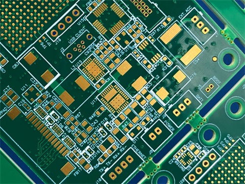
Immersion Gold surface finish provides excellent flatness, solderability, and wire-bond capability. It protects copper circuits from oxidation and ensures reliable soldering even after long-term storage. Green solder mask offers insulation, protection against dust and moisture, and resistance to chemical cleaning. White silkscreen ensures clear component marking, polarity indication, and test point identification. The combination delivers excellent visual inspection compatibility and supports AOI verification.
Application Fields
This 8-layer heavy-copper PCB is intended for high-power and high-reliability scenarios:
TU-865 Copper Clad Laminate (CCL) Technical Knowledge
Material Introduction
TU-865 is a halogen-free high-Tg epoxy resin-based copper clad laminate reinforced with E-glass fabric. It is formulated with phosphorus-nitrogen flame retardant to achieve UL94 V-0 without halogens, antimony, or red phosphorus. Developed for harsh environments and high-reliability electronics, it combines excellent thermal performance, electrical stability, chemical resistance, dimensional stability, and CAF resistance. TU-865P is the matching prepreg for multilayer PCB fabrication.
Key Advantages
Industry Approvals
Standard Specifications
Typical Properties of TU-865 Laminate
|
Property |
Condition |
Typical Value |
IPC-4101 /130 Requirement |
|
Thermal Properties |
|||
|
Tg (DMA) |
— |
220°C |
>170°C |
|
Tg (DSC) |
— |
200°C |
— |
|
Tg (TMA) |
— |
185°C |
— |
|
Td (TGA) |
— |
370°C |
>340°C |
|
CTE x-axis |
— |
11–15 ppm/°C |
— |
|
CTE y-axis |
— |
11–15 ppm/°C |
— |
|
CTE z-axis |
— |
1.80% |
<3.0% |
|
Solder Float 288°C |
— |
>60 sec |
>10 sec |
|
T260 |
— |
>60 min |
>30 min |
|
T288 |
— |
>60 min |
>15 min |
|
T300 |
— |
>30 min |
>2 min |
|
Flammability |
— |
UL94 V-0 |
V-0 |
|
Electrical Properties |
|||
|
Permittivity 1GHz |
RC50% |
4.3–4.6 |
— |
|
Permittivity 10GHz |
RC50% |
4.4 |
— |
|
Loss Tangent 1GHz |
RC50% |
0.010–0.013 |
— |
|
Loss Tangent 10GHz |
RC50% |
0.014 |
— |
|
Volume Resistivity |
C-96/35/90 |
>1×10¹⁰ MΩ·cm |
>1×10⁶ MΩ·cm |
|
Surface Resistivity |
C-96/35/90 |
>1×10⁸ MΩ |
>1×10⁴ MΩ |
|
Electric Strength |
— |
>40 kV/mm |
>30 kV/mm |
|
Dielectric Breakdown |
— |
>50 kV |
>40 kV |
|
Mechanical & Physical |
|||
|
Flexural Strength (length) |
— |
>60,000 psi |
>60,000 psi |
|
Flexural Strength (cross) |
— |
>50,000 psi |
>50,000 psi |
|
Peel Strength (1oz Cu) |
— |
6–9 lb/in |
>4 lb/in |
|
Water Absorption |
E-1/105+D--24/23 |
0.13% |
<0.8% |
Material Summary
TU-865 is a high-performance halogen-free CCL designed for high-reliability PCBs exposed to extreme thermal, chemical, and humidity conditions. Its balanced thermal, electrical, and mechanical properties make it the preferred choice for automotive, server, telecom, and harsh-environment applications. When used in 10oz heavy-copper designs, it provides exceptional current capacity, thermal dissipation, and long-term reliability.
Previous:
6-layer Isola 370HR High-Tg FR-4 PCB 2μ" ENIG Impedance ControlledNext:
4-Layer Rogers RO3210 + RO4450F PCB ISIG Surface Finish 1.321mm With Blind ViaIf you have questions or suggestions,please leave us a message,we will reply you as soon as we can!
Categories
New Products
Wangling F4BTMS220 2-Layer DK2.2 PCB 10 mil Core with Immersion Gold
Wangling F4BTME350 10mil DK3.5 High Frequency Substrate PCB 2-Layer Immersion Gold
Wangling F4BTM300 Custom 2-layer PCB 20mil DK3.0 Substrate with Immersion Gold
Rogers 20mil RT/duroid 6202 2-layer ENIG High-Frequency Microwave PCB
Rogers 20mil AD250C PCB Pure Gold High-Frequency Antenna Circuit Board
8-Layer Hybrid RF PCB: RO4350B + TG170 FR-4 + RO4003C with RO4450F Bondply
4-Layer Rogers RO3010 Hybrid PCB Immersion Silver 2.8mm Finished Thickness
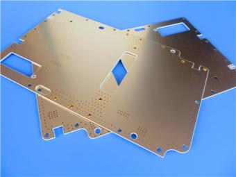
4-Layer 20mil Rogers RO3210 ISIG High-Frequency PCB with Controlled Depth Milling
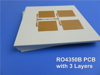
Multilayer high frequency PCBs are made from all high frequency material inclusive of prepreg adhesive.
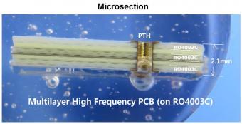
5 layer PCB is fabricated on 3 cores of RO4003C and etched 1 layer copper off to achieve 5 layers.
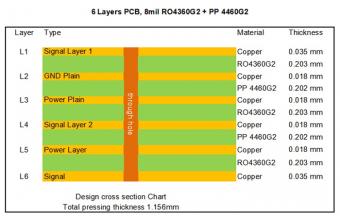
RO4360G2 laminates extend Rogers' portfolio of high performance materials by providing customers with a product that is lead-free process capable and offers better rigidity for improved processability in multi-layer board constructions, while reducing material and fabrication costs.
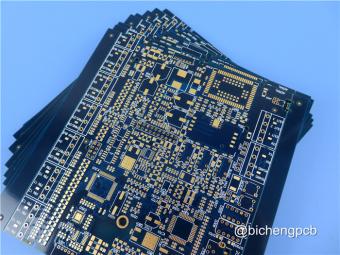
Megtron 6 is an ultra-low loss, highly heat resistant circuit board material designed for mobile, networking, and wireless applications etc.
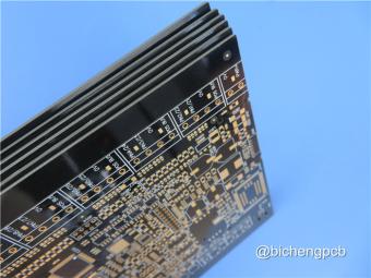
This type of 4-layer circuit board is built on Panasonic Megtron6 (M6) R-5775G high speed low loss material.
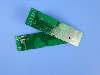
TU-768 / TU-768P laminate / prepreg are made of high quality woven E-glass coated with the epoxy resin system, which provides the laminates with UV-block characteristic, and compatibility with automated optical inspection (AOI) process.
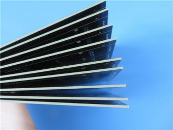
IT-180ATC is an advanced high Tg (175℃ by DSC) multifunctional filled epoxy with high thermal reliability and CAF resistance.
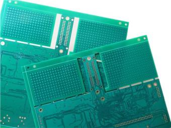
This is a type of 8-layer printed circuit board built on FR-4 Tg175℃ substrate for the application of Satellite Radio.
 6-11C Shidai Jingyuan, Fuyong, Baoan, Shenzhen, Guangdong, China 518103


For inquiries about our products or pricelist, please leave to us and we will be in touch within 24 hours.
© Copyright: 2026 Shenzhen Bicheng Electronics Technology Co., Ltd.. All Rights Reserved.

IPv6 network supported


