

 Call Us Now !
Tel : +86 755 27374946
Call Us Now !
Tel : +86 755 27374946
 Order Online Now !
Email : info@bichengpcb.com
Order Online Now !
Email : info@bichengpcb.com
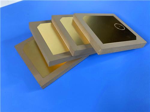
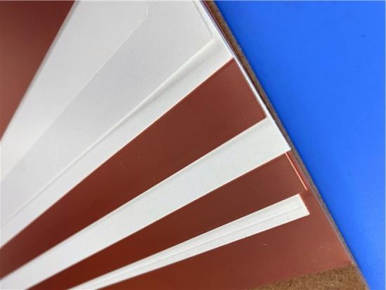
The TP2200 high frequency PCB is a focused high-Dk RF board: two-layer, single-core construction on a controlled Dk 22.0 ceramic–PPO thermoplastic, 1 oz copper, a flat ENIG finish, no mask or silkscreen, and full electrical verification.
Item NO.:
BIC-634-v718Order(MOQ):
1-10Payment:
T/TProduct Origin:
ChinaShipping Port:
ShenzhenLead Time:
7-10 days
Wangling TP2200 PCB 0.8mm Substrate Immersion Gold 2-Layer High-Dk (Dk 22) RF Board
Product Description & TP2200 CCL Material Guide
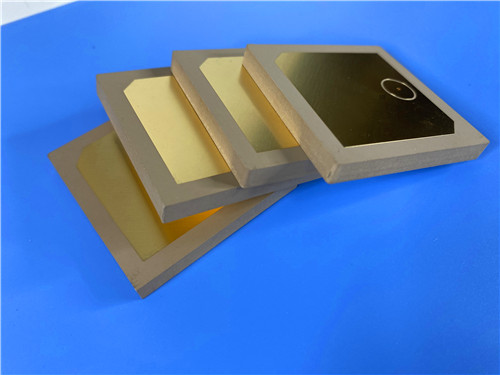
The TP2200 PCB 0.8mm Substrate Immersion Gold is a two-layer rigid RF board built on Wangling TP2200, a glass-fabric-free ceramic-filled PPO thermoplastic with a Dk of 22.0 ± 0.88 at 5 GHz — among the highest dielectric constants in a machinable copper-clad laminate. Its 0.8 mm core carries 1 oz copper, a flat immersion-gold finish, no solder mask or silkscreen, one net and 100% electrical test to IPC Class 2. It is built for compact, dielectric-loaded antennas and defence RF modules where size reduction matters more than routing density; Part 1 describes the board and Part 2 explains the TP2200 CCL.
Part 1 — The TP2200 PCB
1.1 Product Design and Application
A specialized microwave substrate board rather than a general interconnect PCB, its 35.65 × 87 mm strip-like outline, single 0.8 mm high-Dk core and two copper layers suit planar and dielectric-loaded RF structures: miniaturized patch and on-board antennas, Beidou navigation front-ends, missile-borne circuits, fuze electronics and other size-constrained high-frequency assemblies. With one net, 22 through-hole pads and seven top SMT pads, it carries a single RF/feed network rather than a dense component population.
1.2 PCB Construction Details
The table below summarizes the as-built construction, from base material to finish and inspection.
Table 1. PCB construction details.
|
Parameter |
Specification |
|
Base material |
Wangling TP2200 (ceramic-filled PPO, no glass fabric) |
|
Layer count |
2, double sided |
|
Board dimensions |
35.65 × 87 mm, 1 PCS, ±0.15 mm |
|
Minimum trace / space |
4 / 7 mil |
|
Minimum hole size |
0.4 mm |
|
Blind / buried vias |
None |
|
Finished board thickness |
0.9 mm (nominal) |
|
Finished copper weight |
1 oz (1.4 mil / 35 µm), outer layers |
|
Via plating thickness |
20 µm |
|
Surface finish |
Immersion gold (ENIG) |
|
Top silkscreen |
No |
|
Bottom silkscreen |
No |
|
Top solder mask |
No |
|
Bottom solder mask |
No |
|
Electrical test |
100% tested |
|
Artwork format |
Gerber RS-274-X |
|
Quality standard |
IPC Class 2 |
|
Availability |
Worldwide |
1.3 PCB Stackup
The two-layer stackup places the entire RF network on one homogeneousTP2200 core.
Table 2. Two-layer PCB stackup.
|
Layer |
Material |
Thickness |
|
Copper Layer 1 (top) |
Electrodeposited copper |
35 µm |
|
Core |
Wangling TP2200 |
0.8 mm |
|
Copper Layer 2 (bottom) |
Electrodeposited copper |
35 µm |
|
Finished board thickness |
— |
0.9 mm (nominal) |
At 0.8 mm, the core is the thinnest standard thickness Wangling supplies for Dk grades above 10.2; the 0.9 mm nominal finished thickness is the core plus two 35 µm copper layers. A Dk-22 dielectric shortens guided wavelength to roughly 1/√22 of free space — about 21% — so a radiator occupies only a small fraction of the area of the same antenna on conventional laminates, which is why both material and stackup are chosen.
1.4 PCB Statistics
The statistics describe a compact, single-sided RF assembly on one net.
Table 3. PCB statistics.
|
Parameter |
Value |
|
Components |
34 |
|
Total pads |
29 |
|
Thru-hole pads |
22 |
|
Top SMT pads |
7 |
|
Bottom SMT pads |
0 |
|
Vias |
16 |
|
Nets |
1 |
1.5 Surface Finish, Quality and Test
Immersion gold (ENIG) deposits a thin gold layer over a nickel barrier, giving a flat, oxidation-resistant surface for the seven top SMT pads and the through-hole terminations. Its coplanarity suits precise RF alignment, and gold tolerates storage and the low-temperature hand-soldering profile TP2200 requires — wave soldering and high-temperature reflow are outside the material’s limits (Part 2). Via barrels are plated to 20 µm, and every board passes 100% electrical test to IPC Class 2.
1.6 PCB Conclusion
The TP2200 high frequency PCB is a focused high-Dk RF board: two-layer, single-core construction on a controlled Dk 22.0 ceramic–PPO thermoplastic, 1 oz copper, a flat ENIG finish, no mask or silkscreen, and full electrical verification.
It is a purpose-built platform for miniaturized antennas and Beidou, missile-borne and fuze electronics, delivering size reduction that FR-4 and mid-Dk laminates cannot.
Part 2 — CCL Material Knowledge: Wangling TP2200
Part 1 covered the board; this part covers the underlying copper-clad laminate (CCL): composition, complete data sheet, performance, available forms and fabrication rules.
2.1 What the TP Series Is
The Wangling TP series is ahigh-frequency thermoplastic laminate: its dielectric layer is formed from ceramic filler and polyphenylene oxide (PPO) resin with no glass-fabric reinforcement. By adjusting the ceramic-to-PPO ratio, Wangling controls Dk precisely across 3.0–25. The naming denotes the form — TP is unclad smooth material, TP-1 single-sided copper-clad and TP-2 double-sided copper-clad; the Part 1 board uses double-sided TP-2 in the TP2200 grade (Dk 22). Unlike vacuum-metallized ceramics, the ED copper foil is laminated for a far stronger bond, and sheets can be drilled, turned, ground, sheared and etched on standard PCB equipment — a decisive advantage over brittle ceramics.
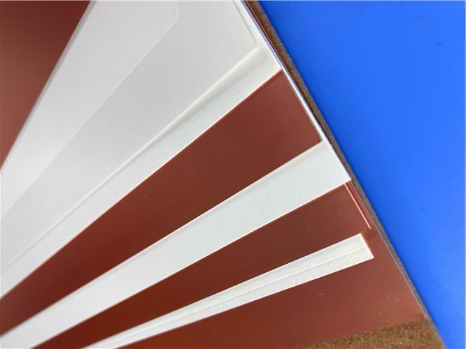
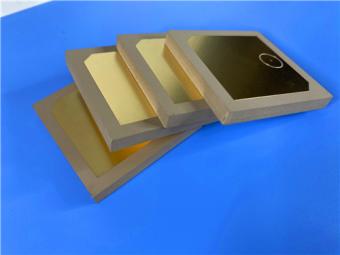
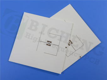
Figure 1. Wangling TP2200 copper-clad laminate: white ceramic–PPO dielectric clad with ED copper foil.
2.2 TP2200 Complete Data Sheet
The complete TP2200 data sheet follows, consolidated from the Wangling material data.
Table 4. TP2200 complete data sheet (typical values; for material selection, not guaranteed limits).
|
Property |
Condition |
Value |
Unit |
Test method |
||||
|
ELECTRICAL PROPERTIES |
|
|
|
|
||||
|
Dielectric constant (Dk) |
5 GHz, Z axis |
22.0 ± 0.88 |
— |
GB/T 12636-1990 / IPC-TM-650 2.5.5.5 stripline |
||||
|
Dk tolerance |
— |
±4% |
— |
Manufacturer |
||||
|
Customizable Dk range |
— |
3.0 – 25 |
— |
Manufacturer |
||||
|
Dissipation factor (Df) |
5 GHz |
0.0020 – 0.0025 |
— |
IPC-TM-650 2.5.5.5 |
||||
|
Dk temperature coefficient (TCDk) |
−55 to +150 °C |
−55 |
ppm/°C |
IPC-TM-650 |
||||
|
Volume resistivity |
500 V, normal state |
> 1 × 10⁹ |
MΩ·cm |
IPC-TM-650 / GB/T 4722-2017 |
||||
|
Surface resistance |
500 V, normal state |
> 1 × 10⁷ |
MΩ |
IPC-TM-650 / GB/T 4722-2017 |
||||
|
THERMAL AND PHYSICAL PROPERTIES |
|
|
|
|
||||
|
Long-term operating temperature |
Thermal chamber |
−100 to +150 |
°C |
Manufacturer |
||||
|
CTE — X / Y |
−55 to +150 °C |
35 / 35 |
ppm/°C |
IPC-TM-650 |
||||
|
CTE — Z |
−55 to +150 °C |
40 |
ppm/°C |
IPC-TM-650 |
||||
|
Thermal conductivity |
— |
0.90 |
W/(m·K) |
Manufacturer |
||||
|
Water absorption |
20 ± 2 °C, 24 h |
≤ 0.01 |
% |
IPC-TM-650 / GB/T 4722-2017 |
||||
|
Density |
TP2200 grade |
2.77 |
g/cm³ |
Manufacturer |
||||
|
MECHANICAL AND FOIL PROPERTIES |
|
|
|
|
||||
|
Peel strength |
1 oz Cu, normal state |
> 0.6 |
N/mm |
IPC-TM-650 |
||||
|
Peel strength |
1 oz Cu, after damp heat |
> 0.4 |
N/mm |
IPC-TM-650 |
||||
|
Copper foil |
Electrodeposited (ED) |
0.018 or 0.035 |
mm |
Manufacturer |
||||
|
Material composition |
— |
PPO resin + ceramic, no glass fabric, ED foil |
— |
Manufacturer |
||||
|
Environmental behaviour |
— |
Radiation resistant; low outgassing |
— |
Manufacturer |
||||
Dk is measured in the Z direction by the stripline method (GB/T 12636-1990 or IPC-TM-650 2.5.5.5); other properties follow IPC-TM-650 or GB/T 4722-2017. All values are typical measurement data for material selection, not guaranteed limits; customers must validate each application.
2.3 Electrical Performance and Differentiation
TP2200 combines an unusually high Dk (22.0 ± 0.88 at 5 GHz, ±4% tolerance) with a low loss tangent of 0.0020–0.0025; loss rises with frequency but changes little below 10 GHz. The payoff is miniaturization: guided wavelength scales with 1/√Dk, so a TP2200 radiator is about 21% of the free-space linear dimension and roughly 45% that of the same design on 4.4-Dk FR-4. A −55 ppm/°C TCDk keeps resonance stable across −55 to +150 °C, and volume resistivity above 10⁹ MΩ·cm maintains insulation. The trade-off is honest: very high Dk narrows antenna bandwidth, so the grade targets fixed-frequency, size-driven defence and navigation designs rather than wideband systems.
2.4 Thermal, Mechanical and Physical Behaviour
TP2200 operates from −100 °C to +150 °C with excellent low-temperature tolerance, and is radiation resistant with low outgassing for vacuum and exposed defence environments. CTE is 35, 35 and 40 ppm/°C in X, Y and Z — higher than copper but isotropic and predictable in a thin 0.8 mm core with 20 µm plated barrels. Water absorption of ≤0.01% (24 h at 20 ± 2 °C) means Dk barely shifts with humidity; density is 2.77 g/cm³ and thermal conductivity 0.90 W/(m·K), slightly above most PTFE laminates. Peel strength exceeds 0.6 N/mm (1 oz foil, normal) and 0.4 N/mm after damp heat — the durable bond vacuum-coated ceramics cannot match.
2.5 Available Thicknesses, Panel Sizes and Forms
TP2200 is offered across a wide thickness range with tight tolerances, standard panel sizes and two ED foil weights.
Table 5. TP2200 standard thicknesses and tolerances.
|
Thickness (mm) |
0.5 |
0.8 |
1.0 |
1.2 |
1.5 |
2.0 |
3.0 |
|
Tolerance (mm) |
±0.04 |
±0.05 |
±0.05 |
±0.05 |
±0.06 |
±0.075 |
±0.10 |
|
Thickness (mm) |
4.0 |
5.0 |
6.0 |
7.0 |
8.0 |
10.0 |
12.0 |
|
Tolerance (mm) |
±0.10 |
±0.12 |
±0.12 |
±0.15 |
±0.18 |
±0.20 |
±0.30 |
The available panel sizes, foil weights, Dk grades and laminate forms are summarized below.
Table 6. TP2200 panel sizes, claddings and forms.
|
Parameter |
Available form |
|
Standard panel sizes |
150 × 150, 160 × 160, 200 × 200, 170 × 240 mm (size tolerance −2 mm) |
|
Copper foil |
ED foil, 0.018 mm (1/2 oz) or 0.035 mm (1 oz) |
|
Minimum thickness |
0.5 mm when Dk ≤ 10.2; 0.8 mm when Dk > 10.2 |
|
Standard Dk grades |
3.0, 4.4, 6.0, 6.15, 9.2, 9.6, 10.2, 11, 16, 20 |
|
Dk customization |
Any value from 3.0 to 25 on request |
|
Laminate forms |
TP unclad smooth; TP-1 single-sided clad; TP-2 double-sided clad |
|
Thickness basis |
Order by total copper-clad thickness or dielectric thickness (state at order) |
2.6 Fabrication, Soldering and Design Rules
TP2200 is processed as a thermoplastic: it machines far more easily than ceramic for high yields and lower cost, supporting drilling, turning, grinding, shearing and etching. Two limits must be respected. First, it is not suited to 260 °C thermal shock and cannot be wave soldered; Wangling recommends hand soldering with a constant-temperature iron, and reflow is generally not advised — if unavoidable, peak set temperature must not exceed 200 °C. Above about 180 °C the material may deform, the foil peel and properties shift. Second, multilayers are not generally recommended; if unavoidable, low-temperature bonding sheets are required. These rules explain why the Part 1 board is a simple two-layer, ENIG-finished design.
2.7 Typical Applications
TP2200 is specified for Beidou navigation systems, missile-borne equipment, fuze electronics and miniaturized antennas.
These share the same requirements: stable very-high-Dk dielectric loading, a wide military-grade temperature range, radiation resistance, low outgassing, and the machining freedom of a thermoplastic rather than a ceramic.
2.8 CCL Conclusion
TP2200 is a differentiated ceramic-filled PPO thermoplastic CCL: a tunable Dk of 3.0–25 delivered at 22.0 ± 0.88 with only 0.0020–0.0025 loss, a −55 ppm/°C TCDk, −100 to +150 °C operation, ≤0.01% water absorption, radiation resistance and low outgassing, plus stronger foil adhesion and easier machining than ceramic. It trades high-temperature assembly and wideband operation for extreme dielectric-loaded miniaturization — exactly why it is the substrate for compact antennas and high-reliability defence and navigation RF.

If you have questions or suggestions,please leave us a message,we will reply you as soon as we can!
Categories
New Products
Wangling TP2200 PCB 0.8mm Substrate Immersion Gold 2-Layer High-Dk (Dk 22) RF Board
Rogers TMM10 PCB 5.08mm Core ENIG 2-Layer High-Dk Microwave Board
Taconic TLX-8 PCB 50mil ENIG 2-Layer High-Frequency RF Circuit Board
Wangling TF440 25mil DK4.4 Laminate Immersion Gold 2-Layer Copper-filling Vias PCB
RO4360G2 Rogers 12mil ENEPIG 2-Layer DK6.15 High Frequency Custom PCB
Wangling F4BTMS220 2-Layer DK2.2 PCB 10 mil Core with Immersion Gold
Wangling F4BTME350 10mil DK3.5 High Frequency Substrate PCB 2-Layer Immersion Gold
Wangling F4BTM300 Custom 2-layer PCB 20mil DK3.0 Substrate with Immersion Gold

RF-10 25mil Taconic PCB Materials stands out as a high-performance solution for RF applications. Its exceptional electrical properties, dimensional stability, thermal conductivity, and adhesion characteristics make it an ideal choice for demanding applications.
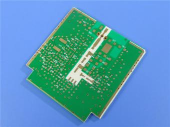
The PCB has a 4-layer hybrid stackup with a 0.5oz+plating ground layer, two 1oz ground layers, and a 0.5oz+plating signal layer.
The dimensions of the board are 55.00 x 26.00 mm, with a tolerance of +/- 0.15mm. The board has 16 components, 26 total pads, 9 through-hole pads, 10 top SMT pads, 7 bottom SMT pads, 77 vias, and 82 nets.
Rogers RO4003C PCB is an innovative and advanced circuit board that is made with high-quality materials.
The RO4350B PCB offers a range of benefits that make it an ideal choice for high-frequency applications. Its low dielectric loss and high thermal conductivity make it perfect for high-frequency applications such as RF and microwave circuits.

Bicheng PCB Ships High-Quality PCBs with Shengyi Tg150 ℃ S1000H Material and Advanced Stackup
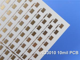
Rogers RO3010 PCB is ideal for a wide range of high-frequency applications, including power amplifiers, filters, couplers, and antennas.
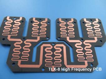
TLX-8 features low dielectric loss, low moisture absorption, and excellent thermal stability, making it ideal for high-frequency and high-speed applications. It has a low dissipation factor, which helps to minimize signal loss and distortion.
 6-11C Shidai Jingyuan, Fuyong, Baoan, Shenzhen, Guangdong, China 518103


For inquiries about our products or pricelist, please leave to us and we will be in touch within 24 hours.
© Copyright: 2026 Shenzhen Bicheng Electronics Technology Co., Ltd.. All Rights Reserved.

IPv6 network supported


