

 Call Us Now !
Tel : +86 755 27374946
Call Us Now !
Tel : +86 755 27374946
 Order Online Now !
Email : info@bichengpcb.com
Order Online Now !
Email : info@bichengpcb.com
This 18-layer high speed PCB is a robust, high-performance interconnect solution engineered from the ground up to solve the complex challenges of modern high-speed digital design.
Item NO.:
BIC-487-v573.0Order(MOQ):
1-10Payment:
T/TProduct Origin:
ChinaShipping Port:
ShenzhenLead Time:
7-10 days
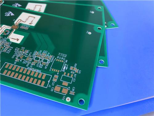
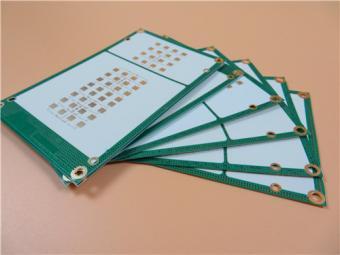
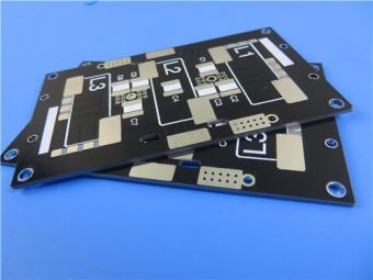
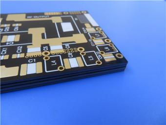
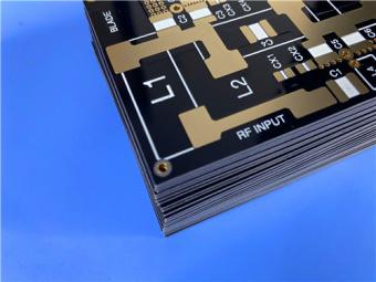
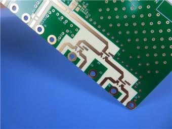
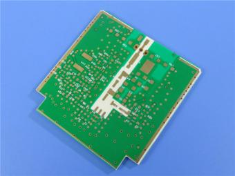
18-layer Panasonic M6 R-5775G High Speed PCB ENIG Via with Resin and Capped
Engineered for the forefront of electronic innovation, this 18-layer printed circuit board represents the pinnacle of high-speed, high-density interconnect technology. Designed to meet the rigorous demands of next-generation computing, telecommunications, and advanced signal processing systems, it leverages state-of-the-art materials and precision manufacturing processes. The core of this board's exceptional performance lies in its sophisticated 18-layer construction utilizing Panasonic's premiumMegtron 6 laminate, enabling unparalleled signal integrity, thermal stability, and reliability in the most challenging operational environments. This product is not merely a circuit board; it is a mission-critical platform engineered to empower groundbreaking technologies.
PCB Construction Details
The following table provides a comprehensive breakdown of the fundamental physical and material specifications that define the board's construction and quality standards.
|
Parameter |
Details |
|
Base Material |
Panasonic Megtron 6 R-5775G (HVLP), Tg 185°C |
|
Layer Count |
18 Layers |
|
Board Dimensions |
240mm x 115mm (1 PCS) |
|
Board Thickness |
2.013mm |
|
Inner Layer Cu Weight |
1 oz (35µm) |
|
Outer Layer Cu Weight |
1 oz (35µm) |
|
Finished Surface Finish |
Electroless Nickel Immersion Gold (ENIG) |
|
Gold Thickness & Coverage Area |
2 µ-inch (Min.), Coverage Area 29% |
|
Solder Mask |
Matte Green |
|
Silkscreen/Legend |
White |
|
Special Processes |
Via Plugging with resin and capped (1 time) |
|
Shipment Inspection |
100% Electrical Test prior to shipment |
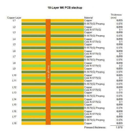
18-Layer M6 High-Speed PCB Stack-up
The stack-up is a symmetrical, tightly controlled structure designed for optimal signal integrity, power delivery, and manufacturability, as detailed in the table below.

Introduction to Megtron 6 Material
Panasonic Megtron 6 is a premier, ultra-low loss laminate and prepreg system specifically engineered for high-speed digital and RF applications. Its key performance advantages include:
1) Extremely Low Dielectric Constant (Dk) and Dissipation Factor (Df):Megtron 6 provides a stable, low Dk (~3.6) and an exceptionally low Df (0.002 @ 10 GHz), which is critical for minimizing signal attenuation and preserving signal integrity at multi-gigabit data rates.
2) Superior Thermal Reliability: With a high Glass Transition Temperature (Tg) of 185°C and excellent thermal decomposition resistance (Td > 400°C), it ensures long-term reliability under high thermal stress, such as during multiple lead-free assembly cycles.
3) Low Hydrophilic (HVLP) Copper Foil: The use of HVLP (Hyper Very Low Profile) copper on the laminate surface results in a smoother conductor, significantly reducing signal loss due to skin effect at high frequencies compared to standard foils.
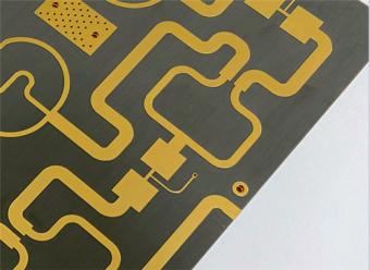
What is a High-Speed PCB?
A High-Speed PCB is not solely defined by a high clock frequency. It is a board where signal integrity considerations—such as impedance control, crosstalk, propagation delay, and transmission line effects—fundamentally dictate the physical design (layout, stack-up, and material selection). When the edge rate (rise/fall time) of a signal is fast enough that the physical length of the interconnect trace becomes a significant fraction of the signal's wavelength, the PCB must be treated as a "high-speed" assembly. At this point, traces behave like transmission lines, and factors like dielectric material properties (Dk/Df) and precise stack-up geometry become paramount to prevent signal degradation, reflections, and timing errors.
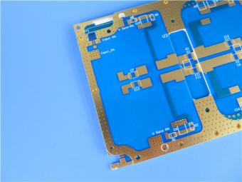
Applications
This 18-layer Megtron 6 PCB is ideally suited for the most demanding technological frontiers:
In summary, this 18-layer high speed PCB is a robust, high-performance interconnect solution engineered from the ground up to solve the complex challenges of modern high-speed digital design. It delivers the signal integrity, power integrity, and thermal resilience required to bring tomorrow's most advanced electronic systems to life.


Previous:
Wangling F4BTMS615 PCB Double-layer 0.254mm 10mil Thick Immersion Tin Bare CopperNext:
16-layer S1000-2M TG180 FR-4 Material 3oz Heavy Copper PCB With HASL LFIf you have questions or suggestions,please leave us a message,we will reply you as soon as we can!
Categories
New Products
Wangling 5mil 0.127mm TFA300 Core 2-layer Immersion Gold Green Solder Mask PCB
7.5mil AGC Taconic TLY-5 Substrate Custom PCB EPIG Finish Bare Copper
10mil Rogers CuClad 250 Immersion Gold 2-Layer Rigid Microwave PCB
20mil F4BTMS450 Wangling DK4.5 Laminate Custom PCB HASL LF Finsh
F4BME275 Wangling DK2.75 Laminate 2-Layer 1.6mm Pure Gold RF Custom PCB
Wangling F4BTD350S High Frequency PCB 2-layer 20mil Thick ENIG DK3.5 Substrate
12-layer TG200 TU-872 SLK High-Speed FR4 1.68mm PCB with ENIG Impedance Control
12-Layer RO4350B + RO3010 3.14mm Hybrid PCB Nickel-Free EPIG Surface Finish Blind Via

RF-10 25mil Taconic PCB Materials stands out as a high-performance solution for RF applications. Its exceptional electrical properties, dimensional stability, thermal conductivity, and adhesion characteristics make it an ideal choice for demanding applications.
The PCB has a 4-layer hybrid stackup with a 0.5oz+plating ground layer, two 1oz ground layers, and a 0.5oz+plating signal layer.
The dimensions of the board are 55.00 x 26.00 mm, with a tolerance of +/- 0.15mm. The board has 16 components, 26 total pads, 9 through-hole pads, 10 top SMT pads, 7 bottom SMT pads, 77 vias, and 82 nets.
Rogers RO4003C PCB is an innovative and advanced circuit board that is made with high-quality materials.
The RO4350B PCB offers a range of benefits that make it an ideal choice for high-frequency applications. Its low dielectric loss and high thermal conductivity make it perfect for high-frequency applications such as RF and microwave circuits.
Bicheng PCB Ships High-Quality PCBs with Shengyi Tg150 ℃ S1000H Material and Advanced Stackup
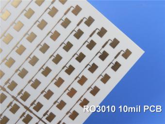
Rogers RO3010 PCB is ideal for a wide range of high-frequency applications, including power amplifiers, filters, couplers, and antennas.
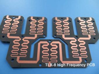
TLX-8 features low dielectric loss, low moisture absorption, and excellent thermal stability, making it ideal for high-frequency and high-speed applications. It has a low dissipation factor, which helps to minimize signal loss and distortion.
 6-11C Shidai Jingyuan, Fuyong, Baoan, Shenzhen, Guangdong, China 518103


For inquiries about our products or pricelist, please leave to us and we will be in touch within 24 hours.
© Copyright: 2026 Shenzhen Bicheng Electronics Technology Co., Ltd.. All Rights Reserved.

IPv6 network supported


