

 Call Us Now !
Tel : +86 755 27374946
Call Us Now !
Tel : +86 755 27374946
 Order Online Now !
Email : info@bichengpcb.com
Order Online Now !
Email : info@bichengpcb.com
For this high-reliability F4BTMS615 high frequency PCB, trust in the material science and process control that meets the stringent demands of modern aerospace and RF engineering.
Item NO.:
BIC-500-v585.0Order(MOQ):
1-10Payment:
T/TProduct Origin:
ChinaShipping Port:
ShenzhenLead Time:
7-10 days
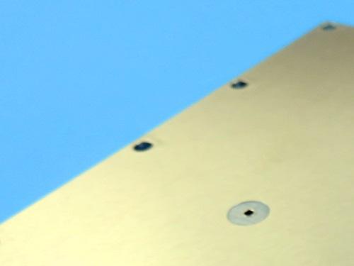
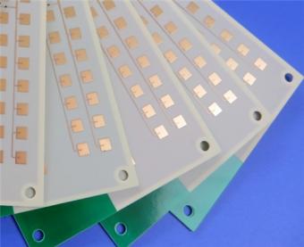
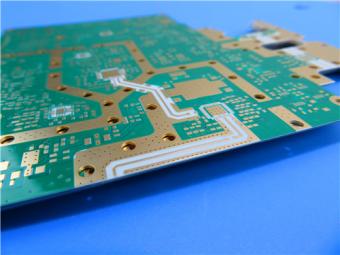
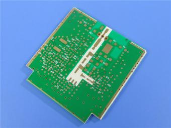
Wangling F4BTMS615 PCB Double-layer 0.254mm 10mil Thick ImmersionTin Bare Copper
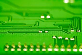
This product is a precision-engineered, double-layer printed circuit board fabricated on the advanced F4BTMS615 ceramic-filled PTFE composite material. Designed for high-reliability radio frequency (RF), microwave, and aerospace applications, this Wangling board exemplifies a perfect synergy between cutting-edge substrate technology and exacting manufacturing standards. The 0.3mm overall thickness and the absence of solder mask and silkscreen indicate a design optimized for controlled impedance, minimal dielectric loss, and potentially complex assembly integration where space and weight are at a premium. The immersion tin surface finish PCB provides a flat, solderable surface excellent for fine-pitch components and offers superior shelf life compared to bare copper.
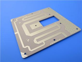
PCB Construction
The F4BTMS615 PCB construction details are summarized below, highlighting its key dimensional and manufacturing specifications:
|
PCB Construction Details |
Specification |
|
Board Dimensions |
45.8 mm x 102.1 mm =1PCS |
|
Dimensional Tolerance |
±0.15 mm |
|
Minimum Trace / Space |
4 mil / 5 mil |
|
Minimum Finished Hole Size |
0.3 mm |
|
Via Type |
Through-Hole Only (No Blind Vias) |
|
Finished Board Thickness |
0.3 mm |
|
Finished Copper Weight (Outer Layers) |
1 oz (35 μm / ~1.4 mils) |
|
Via Plating Thickness |
20 μm |
|
Surface Finish |
Immersion Tin |
|
Top / Bottom Silkscreen |
No |
|
Top / Bottom Solder Mask |
No |
|
Electrical Test |
100% Test Prior to Shipment |
PCB Stackup (2-Layer Rigid)
The 10mil F4BTMS615 PCB stackup is a simple yet high-performance two-layer structure, as detailed in the following table:
|
Layer |
Material |
Thickness |
|
Layer 1 |
Copper Foil |
35 μm (1 oz) |
|
Core |
F4BTMS615 Dielectric |
0.254 mm (10 mil) |
|
Layer 2 |
Copper Foil |
35 μm (1 oz) |
PCB Statistics
A statistical overview of the board's design complexity and component layout is provided here:
|
PCB Statistics |
Quantity |
|
Total Components |
18 |
|
Total Pads |
42 |
|
Through-Hole Pads |
15 |
|
Surface-Mount (SMT) Pads - Top Side |
27 |
|
Surface-Mount (SMT) Pads - Bottom Side |
0 |
|
Total Vias |
35 |
|
Total Nets |
2 |
Advanced Material Foundation: F4BTMS615
This PCB is built upon the innovative F4BTMS615 substrate, a significant upgrade from standard PTFE materials. It represents a technological breakthrough, formulated with a high loading of special nano-ceramics uniformly dispersed within a polytetrafluoroethylene (PTFE) resin matrix and reinforced with ultra-thin, ultra-fine glass fiber cloth. This proprietary formulation drastically reduces the negative effects of traditional glass weave on signal propagation, minimizing dielectric loss and improving dimensional stability. The result is a material with remarkably low and consistent anisotropy across the X, Y, and Z axes. It comes standard with RTF (Reverse Treated Foil) low-profile copper, which reduces conductor loss at high frequencies while maintaining excellent peel strength.

Key Material Features & Electrical Properties
The F4BTMS615 Wangling substrate delivers exceptional performance parameters critical for high-frequency designs:
1)Stable Dielectric Constant: A consistent Dk of 6.15 at 10GHz ensures predictable impedance control.
2)Ultra-Low Loss: An extremely low dissipation factor (Df) of 0.0020 at 10GHz (0.0023 at 20GHz) minimizes signal attenuation.
3)Excellent Dimensional & Thermal Stability: Very low Coefficient of Thermal Expansion (CTE: 10/12/40 ppm/°C in X/Y/Z) and a low thermal coefficient of Dk (-96 ppm/°C) ensure reliable performance under thermal cycling.
4)Enhanced Thermal Management: High thermal conductivity of 0.67 W/mK aids in heat dissipation from active components.
5)High Reliability: Low moisture absorption (0.1%) and a wide operating temperature range ensure robustness in harsh environments.
Typical Applications
This combination of a precisely manufactured thin PCB and the high-performance Wangling F4BTMS615 substrate makes it ideal for advanced electronic systems, including:
Ordering & Documentation
This product is available for global procurement. All fabrication data is supplied in the industry-standard Gerber RS-274-X format, ensuring seamless and accurate manufacturing. For this high-reliability F4BTMS615 high frequency PCB, trust in the material science and process control that meets the stringent demands of modern aerospace and RF engineering.


Previous:
Rogers Cuclad 217 20mil laminate PCB Double-layer Immersion Gold Blue Solder MaskNext:
18-layer Panasonic M6 R-5775G High Speed PCB ENIG Via with Resin and CappedIf you have questions or suggestions,please leave us a message,we will reply you as soon as we can!
Categories
New Products
2-Layer 20mil FSD1020T ENIG High-Frequency PCB with Via Resin Plugged and Capped
4-Layer F4BM265+S1000-2M Material Hyrbid PCB with Blind Via Impedance Control & ENIG
4-Layer Wangling WL-CT338 + FR4 Hybrid PCB ENIG Green Solder Mask White Silkscreen
6-layer Isola 370HR High-Tg FR-4 PCB 2μ" ENIG Impedance Controlled
6-Layer RO4003C + FR4 Mixed Dielectric PCB with Hard Gold Plating Blind Via
30mil Taconic CER-10 2-layer Immersion Silver DK10 High Frequency Laminate PCB
31mil Rogers RT/duroid 5880 Double-sided Bare Copper ENIG Finished PCB
Wangling TFA294 Laminate 40mil Immersion Silver No Solder Mask Silkscreen Custom PCB

RF-10 25mil Taconic PCB Materials stands out as a high-performance solution for RF applications. Its exceptional electrical properties, dimensional stability, thermal conductivity, and adhesion characteristics make it an ideal choice for demanding applications.
The PCB has a 4-layer hybrid stackup with a 0.5oz+plating ground layer, two 1oz ground layers, and a 0.5oz+plating signal layer.
The dimensions of the board are 55.00 x 26.00 mm, with a tolerance of +/- 0.15mm. The board has 16 components, 26 total pads, 9 through-hole pads, 10 top SMT pads, 7 bottom SMT pads, 77 vias, and 82 nets.
Rogers RO4003C PCB is an innovative and advanced circuit board that is made with high-quality materials.
The RO4350B PCB offers a range of benefits that make it an ideal choice for high-frequency applications. Its low dielectric loss and high thermal conductivity make it perfect for high-frequency applications such as RF and microwave circuits.
Bicheng PCB Ships High-Quality PCBs with Shengyi Tg150 ℃ S1000H Material and Advanced Stackup
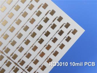
Rogers RO3010 PCB is ideal for a wide range of high-frequency applications, including power amplifiers, filters, couplers, and antennas.
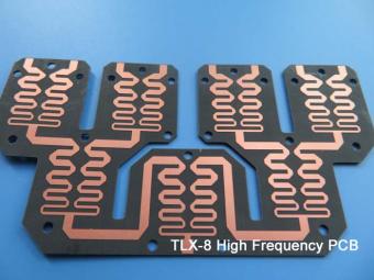
TLX-8 features low dielectric loss, low moisture absorption, and excellent thermal stability, making it ideal for high-frequency and high-speed applications. It has a low dissipation factor, which helps to minimize signal loss and distortion.
 6-11C Shidai Jingyuan, Fuyong, Baoan, Shenzhen, Guangdong, China 518103


For inquiries about our products or pricelist, please leave to us and we will be in touch within 24 hours.
© Copyright: 2026 Shenzhen Bicheng Electronics Technology Co., Ltd.. All Rights Reserved.

IPv6 network supported


