

 Call Us Now !
Tel : +86 755 27374946
Call Us Now !
Tel : +86 755 27374946
 Order Online Now !
Email : info@bichengpcb.com
Order Online Now !
Email : info@bichengpcb.com
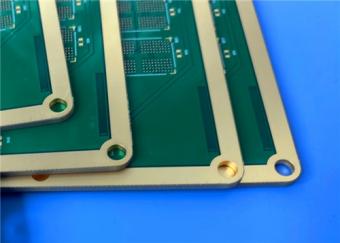
This high-performance 2-layer rigid printed circuit board is purpose-built for demanding radio-frequency, microwave, 5G/6G communication, radar, and aerospace applications.
Item NO.:
BIC-545-v630.0Order(MOQ):
1-10Payment:
T/TProduct Origin:
ChinaShipping Port:
ShenzhenLead Time:
7-10 days
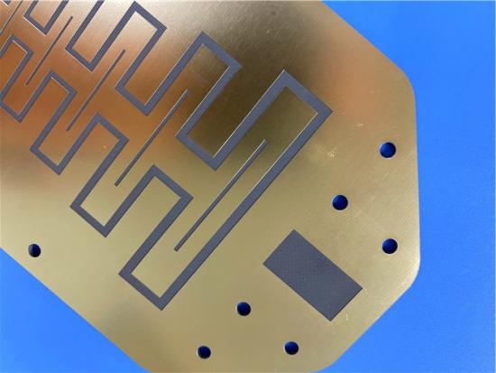
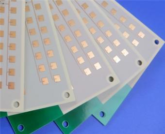
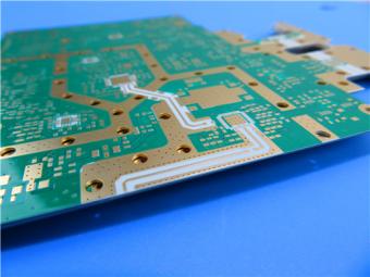
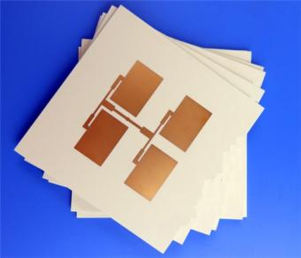
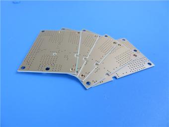
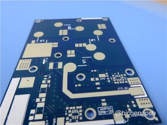
20mil AGC RF-30A 2-Layer High Frequency ENIG Finish Custom PCB
PCB productOverview
This high-performance 2-layer rigid printed circuit board is purpose-built for demanding radio-frequency, microwave, 5G/6G communication, radar, and aerospace applications. Built on AGC's advanced RF-30A organic-ceramic laminate with 20mil dielectric thickness and finished with Electroless Nickel Immersion Gold (ENIG), this AGC PCB delivers exceptional high-frequency signal integrity, low insertion loss, stable electrical performance across wide bandwidths, and robust reliability under lead-free assembly and harsh environmental conditions. Every unit undergoes 100% electrical testing before shipment to ensure compliance with IPC-Class-2 standards and consistent functional performance. This AGC RF-30A PCB combines optimized structural design, precision manufacturing, and industry-leading substrate material to serve high-volume commercial RF systems while maintaining cost-effectiveness and manufacturing scalability.

1. PCB Construction Overview
The following table summarizes the core mechanical, structural, and surface-processing parameters of this 20mil RF-30A PCB, defining its physical form, fabrication limits, and cosmetic specifications.
|
Parameter |
Specification |
|
Base Material |
RF-30A |
|
Layer Count |
2 Layers |
|
Board Dimensions |
85.6 mm x 99.8 mm per piece |
|
Minimum Trace / Space |
4 / 6 mils |
|
Minimum Hole Size |
0.25 mm |
|
Blind Vias |
None |
|
Finished Board Thickness |
0.6 mm |
|
Finished Copper Weight |
1 oz (1.4 mils / 35 µm) on outer layers |
|
Via Plating Thickness |
20 µm |
|
Surface Finish |
Electroless Nickel Immersion Gold (ENIG) |
|
Top Silkscreen |
White |
|
Bottom Silkscreen |
None |
|
Top Solder Mask |
Green |
|
Bottom Solder Mask |
None |
|
Electrical Test |
100% Electrical testing performed prior to shipment |
2. PCB Stackup Structure
This table presents the symmetrical layer stackup, which ensures balanced thermal and mechanical behavior and stable impedance for high-frequency transmission lines.
|
Layer |
Material |
Thickness |
|
Copper Layer 1 (Top) |
Copper |
35 µm (1 oz) |
|
Dielectric Core |
RF-30A Laminate |
0.508 mm (20 mils) |
|
Copper Layer 2 (Bottom) |
Copper |
35 µm (1 oz) |
3. PCB Circuit & Layout Statistics
This table provides key layout and interconnection statistics, supporting assembly planning, impedance control, and manufacturing yield analysis.
|
Parameter |
Count |
|
Components |
54 |
|
Total Pads |
43 |
|
Thru-Hole Pads |
19 |
|
Top SMT Pads |
24 |
|
Bottom SMT Pads |
0 |
|
Vias |
36 |
|
Nets |
2 |
Performance Features and Applications
The combination of RF-30A high frequency laminate and ENIG finish yields measurable benefits:
1)Low & Stable Dielectric Constant (Dk): 3.0±0.05 at 10 GHz–minimal phase shift over temperature and frequency.
2)Low Dissipation Factor (Df): 0.003 at 10 GHz–reduces insertion loss and heating in high-power RF chains.
3)Excellent PIM Performance: Measured below -160 dBc (20W per channel, 800/1800 MHz)–critical for multi-carrier communication systems.
4)High Thermal Reliability: T260 >90 min, T288 >30 min–supports lead-free assembly and repeated rework.
5)Low Moisture Absorption: 0.08%–preserves Dk/Df in humid environments (e.g., outdoor base stations).
6)Matched CTE to Copper: X: 9-11 ppm/°C, Y: 11-13 ppm/°C–minimizes copper trace stress during thermal cycling.
Typical applications include:
-5G/6G base stations and antennas
-Radar systems (phased array, automotive)
-Satellite communication equipment
-RF modules and transceivers (PA, LNA)
-Aerospace and defense electronics
-High-frequency test instruments
-Automotive V2X and radar components
Manufacturing readiness: The design complies with IPC-Class-2, allowing for cost-effective production while maintaining reliable field performance. 100% electrical testing guarantees continuity and isolation before shipment.
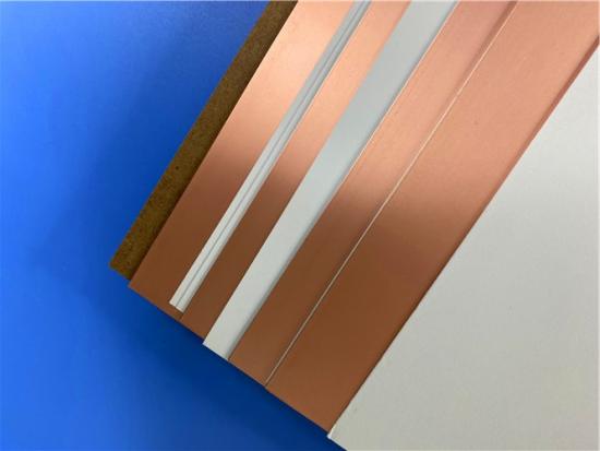
RF-30A CCL Laminate Knowledge Base
*The following section provides an independent, detailed technical reference for AGC RF-30A the core material used in the above 20mil AGC PCB. It includes key benefits, a comprehensive properties table, thickness/panel options, and design guidelines.*
1. Overview and Benefits
RF-30A is an organic-ceramic laminate from AGC family of high-performanceRF substrates. It combines woven glass reinforcement with a proprietary ceramic-filled resin system–bridging the gap between conventional FR-4 (lossy at RF) and pure PTFE (expensive, difficult to process).RF-30A substrate is optimized for low-cost, high-volume commercial microwave and radio frequency applications.
Key Benefits
2. Detailed Properties Table
*All values are typical based on AGC datasheets (IPC-TM-650 test methods). For critical specifications, please contact AGC directly.*
|
Properties |
Conditions |
Typical Value |
Unit |
Test Method |
|
Electrical Properties |
||||
|
Dielectric Constant |
@ 1.9 GHz |
2.97 ± 0.05 |
- |
IPC-TM 650 2.5.5.5.1 mod |
|
Dissipation Factor |
@ 1.9 GHz |
0.0013 |
- |
IPC-TM 650 2.5.5.5.1 mod |
|
@ 10 GHz |
0.002 |
- |
IPC-TM 650 2.5.5.5.1 mod |
|
|
Volume Resistivity |
- |
3.0 x 10⁹ |
Mohm·cm |
|
|
Surface Resistivity |
- |
2.0 x 10⁸ |
Mohms |
|
|
Thermal Properties |
||||
|
Thermal Conductivity |
- |
0.42 |
W/M*K |
IPC-650 2.4.50 |
|
CTE (50-150°C) |
X |
8 |
|
|
|
Y |
11 |
ppm/°C |
IPC-650 2.4.41 |
|
|
Z |
60 |
|
|
|
|
Mechanical Properties |
||||
|
Specific Heat |
|
0.95 |
J/gK |
IPC-650 2.4.50 |
|
Density |
Specific Gravity |
2.16 |
g/cm3 |
IPC-TM-650 2.3.5 |
|
Flexural Strength |
MD |
126.5 (18,000) |
N/mm2 (psi) |
|
|
CD |
119.5 (17,000) |
N/mm2 (psi) |
IPC-650 2.4.19 |
|
|
Tensile Strength |
MD |
133.6 (19,000) |
N/mm2 (psi) |
|
|
CD |
105.5 (15,000) |
N/mm2 (psi) |
IPC-650 2.4.19 |
|
|
Dimensional Stability |
MD |
0.049 |
% (30 mil) |
IPC-650 2.4.39 (After Etch) |
|
0.025 |
% (60 mil) |
|||
|
CD |
0.041 |
% (30 mil) |
||
|
0.026 |
% (60 mil) |
|||
|
MD |
0.049 |
% (30 mil) |
IPC-650 2.4.39 (After Stress) |
|
|
0.019 |
% (60 mil) |
|||
|
CD |
0.031 |
% (30 mil) |
||
|
0.011 |
% (60 mil) |
|||
|
Chemical / Physical Properties |
||||
|
Flammability Rating |
- |
- |
V-0 |
Internal |
3. Typical Thicknesses and Panel Sizes
RF-30A PCB material is available in a range of standard thicknesses and sheet sizes. Custom thicknesses in 0.010" (0.25 mm) increments can be quoted.
|
Inches |
mm |
|
0.02 |
0.51 |
|
0.03 |
0.76 |
|
0.04 |
1.02 |
|
0.06 |
1.52 |
RF-30A PCB substrate is produced in standard thickness increments of 0.010 inch (0.250 mm), supporting flexible PCB stack-up design.
|
Panel Size (Inches) |
Panel Size (mm) |
|
12 × 18 |
305 × 457 |
|
16 × 18 |
406 × 457 |
|
18 × 24 |
457 × 610 |
|
36 × 48 |
914 × 1,220 |
|
|
|
4. Design and Fabrication Guidance
1)Impedance control: Use Dk = 3.0 at your operating frequency (10 GHz recommended). For microstrip, adjust trace width accordingly.
2)PTH reliability: The low Z-axis CTE (60 ppm/°C) allows standard FR-4 drilling and plating parameters. No special desmear needed.
3)Solder assembly: Compatible with lead-free reflow (peak 260°C). The ENIG finish (if specified) provides excellent solder wetting.
4)PIM-sensitive designs: Use very low profile copper and avoid abrupt impedance changes. Ground vias spacing≤ λ/10 at highest frequency.
5)Storage: Keep in original moisture barrier bag. Shelf life 12 months at <30°C / <60% RH.
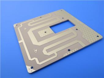
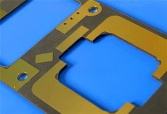
5.Material Image Reference (RF-30A CCL)

6. Summary of RF-30A CCL Value
RF-30A represents AGC's advanced material solution for cost-sensitive, high-volume RF applications that do not compromise on electrical performance. By integrating ceramic fillers for stable dielectric behavior and low loss with woven glass for mechanical strength, it achieves an exceptional price/performance ratio. Its stable PIM, low moisture absorption, controlled CTE, and compatibility with standard PCB manufacturing processes make it the material of choice for modern RF, microwave, and high-frequency designs that demand reliability, consistency, and scalability.


Previous:
30mil RT/Duroid 6002 Double Sided Rogers PCB Immersion Silver Finish Bare CopperNext:
High Performance 4-Layer Polyimide PCB with Matte Black Mask and ENEPIG Surface FinishIf you have questions or suggestions,please leave us a message,we will reply you as soon as we can!
Categories
New Products
2-Layer 20mil FSD1020T ENIG High-Frequency PCB with Via Resin Plugged and Capped
4-Layer F4BM265+S1000-2M Material Hyrbid PCB with Blind Via Impedance Control & ENIG
4-Layer Wangling WL-CT338 + FR4 Hybrid PCB ENIG Green Solder Mask White Silkscreen
6-layer Isola 370HR High-Tg FR-4 PCB 2μ" ENIG Impedance Controlled
6-Layer RO4003C + FR4 Mixed Dielectric PCB with Hard Gold Plating Blind Via
30mil Taconic CER-10 2-layer Immersion Silver DK10 High Frequency Laminate PCB
31mil Rogers RT/duroid 5880 Double-sided Bare Copper ENIG Finished PCB
Wangling TFA294 Laminate 40mil Immersion Silver No Solder Mask Silkscreen Custom PCB
Polytetrafluoroethylene (Short for PTFE), commonly known as "plastic king ", is a polymer compound made of tetrafluoroethylene by polymerization. It has excellent chemical stability, corrosion resistance, sealing, high lubrication and non-viscosity, electrical insulation and good aging resistance.
Rogers TMM4 thermoset microwave material is ceramic, hydrocarbon, thermoset polymer composite designed for high plated-through-hole reliability stripline and microstrip applications.
Taconic TLY laminates are a type of low loss laminates. They are manufactured with very light weight woven fiberglass and are more dimensionally stable than chopped fiber reinforced PTFE composites.
RO3203 laminates combine the surface smoothness of a non-woven PTFE laminate, for finer line etching tolerances, with the rigidity of a woven-glass PTFE laminate. These materials can be fabricated into printed circuit boards using
This type of immersion silver RF PCB is made on one of Taconic’s ORCER family material: RF-45.
Rogers’ TMM10 thermoset microwave materials are ceramic, hydrocarbon, thermoset polymer composites designed for high plated-thru-hole reliability stripline and microstrip applications.
Rogers RO3006 was designed to offer exceptional electrical and mechanical stability at competitive prices.
RT/duroid 6010LM microwave laminates feature ease of fabrication and stability in use. This property results in the possibility of mass production and reducing the cost of goods.
 6-11C Shidai Jingyuan, Fuyong, Baoan, Shenzhen, Guangdong, China 518103


For inquiries about our products or pricelist, please leave to us and we will be in touch within 24 hours.
© Copyright: 2026 Shenzhen Bicheng Electronics Technology Co., Ltd.. All Rights Reserved.

IPv6 network supported


