

 Call Us Now !
Tel : +86 755 27374946
Call Us Now !
Tel : +86 755 27374946
 Order Online Now !
Email : info@bichengpcb.com
Order Online Now !
Email : info@bichengpcb.com
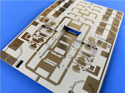
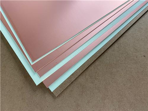
As a mid-range high-frequency ceramic-filled PTFE copper clad laminate in the Rogers RO3000 product line, RO3006 strikes an optimal balance between electrical stability, mechanical reliability and mass-production cost.
Item NO.:
BIC-600-v685.0Order(MOQ):
1-10Payment:
T/TProduct Origin:
ChinaShipping Port:
ShenzhenLead Time:
7-10 days
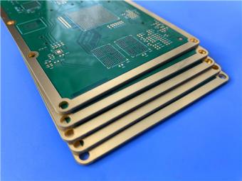
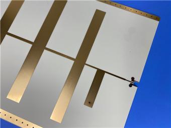
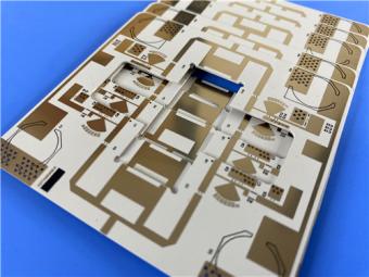
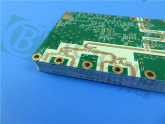
RO3006 PCB 5mil Rogers Substrate 2-layer ENIG Finish No Solder mask
Executive Summary
This presentation delivers an in-depth, data-backed technical introduction to a custom 2-layer rigid high-frequency PCB built on 5mil Rogers RO3006 ceramic-filled PTFE core with ENIG (Electroless Nickel Immersion Gold) surface finish, fully separated into two independent modules: finished PCB assembly product introduction andbase RO3006 Copper Clad Laminate professional material knowledge.
The RO3006 PCB section covers manufacturing specifications via standardized simplified tables, structural stackup, circuit statistics, production standards, differentiated competitive advantages, and targeted RF/microwave application scenarios, ending with a dedicated PCB performance conclusion.
The subsequent CCL chapter provides a complete datasheet parameter table, raw material composition explanation, performance curve interpretation, physical configuration options, and a standalone laminate material conclusion.
Part 1: Finished RO3006 5mil 2-Layer ENIG PCB Product Introduction
1.1 Core Product Brief
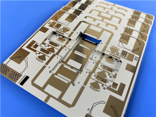
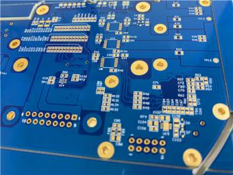
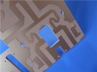
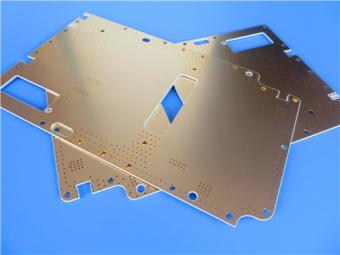
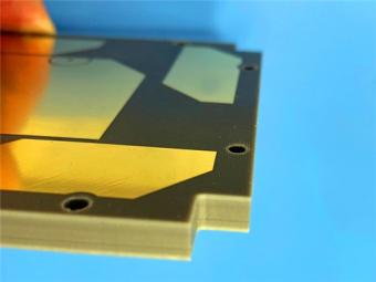
This ultra-thin double-sided RF printed circuit board adopts Rogers RO3006 5mil (0.127mm) high-frequency dielectric substrate, with a final finished board thickness controlled at 0.25mm, 1oz outer copper foil, ENIG surface plating, no blind buried vias, and complies with IPC-Class-2 commercial reliability standards. It is customized for compact microwave signal transmission hardware, with precision fine-line capability of 5mil trace /7mil space, 0.25mm minimum mechanical drill hole, and undergoes 100% full electrical continuity testing before delivery to eliminate open/short circuit defects.
Unlike conventional FR-4 high-frequency boards, this RO3006 PCB eliminates room-temperature dielectric constant step drift via ceramic-filled PTFE formula, paired with ENIG finish to optimize high-frequency soldering, wire bonding and anti-oxidation performance for long-term outdoor and variable-temperature RF equipment.
1.2 PCB Construction Parameter Table
This table aggregates all fixed fabrication dimension, coating and process rules of the finished PCB for quick design verification.
|
Item |
Technical Parameter |
|
Single Board Size |
43.66mm × 28.01mm |
|
Min Trace / Min Space |
5 mil / 7 mil |
|
Minimum Through Hole Diameter |
0.25mm |
|
Via Type |
Only through vias, no blind/buried vias |
|
Final Board Thickness |
0.25mm |
|
Outer Copper Weight |
1 oz (1.4 mil / 35μm) |
|
Via Plating Thickness |
20μm copper plating |
|
Surface Finish |
ENIG (upgrade from original OSP design) |
|
Top Silkscreen |
Black ink |
|
Bottom Silkscreen |
None |
|
Solder Mask |
Top & Bottom: No mask layer |
|
Pre-Shipment Test |
100% electrical continuity test |
|
Accepted Quality Standard |
IPC-Class-2 |
|
Production File Format |
Gerber RS-274-X |
|
Supply Coverage |
Global delivery & support |
1.3 PCB Stackup Layer Structure Table
This table illustrates the symmetrical 2-layer rigid substrate stacking sequence from top to bottom, clearly marking copper thickness and dielectric core thickness.
|
Layer Sequence |
Material & Thickness |
|
Layer 1 (Top Signal Copper) |
35μm electrodeposited copper foil |
|
Dielectric Core |
Rogers RO3006 5mil (0.127mm) ceramic PTFE |
|
Layer 2 (Bottom Signal Copper) |
35μm electrodeposited copper foil |
1.4 PCB Circuit Statistical Table
This table quantifies component pads, vias and net counts to reflect low-complexity dual-circuit RF layout characteristics of this PCB unit.
|
Circuit Statistical Item |
Quantity |
|
Mounted Component Count |
20 |
|
Total Pad Count |
24 |
|
Through-Hole Pads |
13 |
|
Top SMT Pads |
11 |
|
Bottom SMT Pads |
0 |
|
Through Vias |
34 |
|
Independent Signal Nets |
2 |
1.5 Differentiated Competitive Advantages of This PCB
1) Ultra-thin 5mil RO3006 core + 0.25mm finished thickness:
Realizes compact antenna and radar module miniaturization that thick high-frequency substrates cannot match, suitable for narrow cavity device integration.
2) ENIG surface finish upgrade:
Compared with the base OSP process recorded in the original fabrication file, ENIG provides uniform flat gold plating layer, effectively reducing high-frequency insertion loss caused by copper oxidation, supporting both SMT reflow soldering and gold wire bonding for RF amplifier chips; no solder mask eliminates parasitic capacitance interference on microstrip antenna traces.
3) Copper-matched low CTE substrate:
X/Y axis thermal expansion coefficient ofRO3006 material reaches 17ppm/°C, consistent with 1oz copper foil, avoiding pad delamination and trace cracking during repeated thermal cycling of automotive radar and satellite equipment.
4) Stable broadband electrical performance:
Dk 6.15±0.15 at 10GHz with ultra-low Df 0.002, no sudden dielectric constant jump near room temperature as seen in glass-reinforced PTFE boards, ensuring consistent impedance control across -55°C to 288°C operating range.
5) Standardized high-volume manufacturability:
Compatible with mature PTFE PCB mass production workflows, IPC-Class-2 commercial reliability standard balances cost and performance for batch wireless communication equipment, supported by worldwide logistics and technical after-sales service.
1.6 Typical Target Application Scenarios
This 2-layer thin RO3006 ENIG PCB targets commercial microwave and RF hardware with strict signal stability and compact size requirements:
1.7 Conclusion for Finished PCB
This 5mil 2-layer RO3006 PCB with ENIG finish is a balanced, cost-effective high-frequency rigid circuit solution optimized for miniaturized dual-signal RF layouts. Its standardized fine-line fabrication parameters, matched copper-substrate thermal expansion design, oxidation-resistant ENIG plating, and stable ceramic-filled PTFE dielectric core jointly solve two core pain points of traditional RF PCBs: temperature-induced impedance drift and surface oxidation signal attenuation. Compliant with IPC-Class-2 and verified via full electrical testing, it delivers consistent, repeatable performance for medium-volume commercial microwave products, filling the market gap between ultra-thin low-loss high-frequency substrates and affordable mass-producible PCB assemblies.
Part 2: In-Depth Technical Knowledge of RO3006 CCL (Copper Clad Laminate)
2.1 RO3006 CCL Material Overview
Rogers RO3006 belongs to the RO3000 series ceramic-filled PTFE composite copper clad laminates, engineered exclusively for commercial microwave and radio frequency circuits. Unlike glass-fiber reinforced PTFE substrates, its ceramic filler formula suppresses the abnormal Dk step change near room temperature, achieving linear dielectric constant stability over wide temperature and frequency bands. The material maintains uniform mechanical rigidity across all Dk grades in the RO3000 family, enabling hybrid multilayer stacking with FR-4 epoxy glass boards without severe warpage.Rogers3006 supports lead-free reflow soldering processes and UL94 V-0 flame retardant rating, with low moisture absorption and high thermal decomposition temperature to adapt to harsh outdoor and high-power operating environments.
2.2 Complete RO3006 Datasheet Standard Performance Table
All values are typical test data from Rogers official datasheet, tested under specified IPC/ASTM standard conditions:
|
Performance Category |
Parameter |
Typical Value |
Unit |
Test Condition |
Test Standard |
|
Electrical Properties |
Process Dielectric Constant |
6.15 ± 0.15 |
- |
10 GHz, 23°C |
IPC TM-650 2.5.5.5 |
|
Design Dielectric Constant |
6.5 |
- |
8–40 GHz |
Differential Phase Length |
|
|
Dissipation Factor (Df) |
0.002 |
- |
10 GHz, 23°C |
IPC TM-650 2.5.5.5 |
|
|
Thermal Coefficient of Dk |
-262 |
ppm/°C |
-50°C ~ 150°C, 10GHz |
IPC TM-650 2.5.5.5 |
|
|
Volume Resistivity |
10⁵ |
MΩ·cm |
Condition A |
IPC TM-650 2.5.17.1 |
|
|
Surface Resistivity |
10⁵ |
MΩ |
Condition A |
IPC TM-650 2.5.17.1 |
|
|
Thermal & Mechanical |
Decomposition Temperature (Td) |
>500 |
°C |
TGA test |
ASTM D3850 |
|
X-axis CTE |
17 |
ppm/°C |
-55°C ~ 288°C |
IPC TM-650 2.4.41 |
|
|
Y-axis CTE |
17 |
ppm/°C |
-55°C ~ 288°C |
IPC TM-650 2.4.41 |
|
|
Z-axis CTE |
24 |
ppm/°C |
-55°C ~ 288°C |
IPC TM-650 2.4.41 |
|
|
Thermal Conductivity |
0.79 |
W/m·K |
50°C |
ASTM D5470 |
|
|
Copper Peel Strength (1oz EDC) |
7.1 |
lbs/in |
Post solder float |
IPC TM-650 2.4.8 |
|
|
Young’s Modulus |
1498 / 1293 |
MPa |
23°C |
ASTM D638 |
|
|
Dimensional Stability MD/CMD |
1.8 |
mm/m |
Condition A |
IPC TM-650 2.2.4 |
|
|
Environmental & Physical |
Moisture Absorption |
0.02 |
% |
D48/50 |
IPC TM-650 2.6.2.1 |
|
Density |
2.6 |
g/cm³ |
23°C |
ASTM D792 |
|
|
Specific Heat Capacity |
0.86 |
J/g/K |
Calculated value |
N/A |
|
|
Flammability Grade |
V-0 |
- |
N/A |
UL 94 |
|
|
Lead-Free Process Compatibility |
Yes |
- |
N/A |
N/A |
2.3 CCL Physical Configuration Specifications
1) Standard Dielectric Thicknesses:
0.005”(5mil/0.127mm), 0.010”(10mil/0.25mm), 0.025”, 0.050”;
The target PCB uses the thinnest 5mil core for miniaturization.
2) Standard Raw Panel Sizes:
12”×18”(305×457mm), 24”×18”(610×457mm);
Custom sizes available via Rogers sales engineering.
3) Standard Copper Cladding:
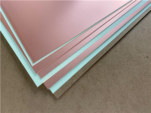
½oz (18μm) and 1 oz (35μm) electrodeposited copper foil, matching the 1oz outer copper design of the finished PCB.
2.4 Core Material Technical Benefits & Design Value
1) Temperature-stable Dk eliminates phase shift:
The ceramic filler eliminates the sharp Dk inflection point of woven PTFE substrates near room temperature, ensuring consistent antenna radiation pattern and filter frequency response in vehicle and outdoor equipment with large temperature swings.
2) Copper-matched in-plane CTE minimizes assembly failure:
X/Y 17ppm/°C expansion matches copper foil deformation rate, reducing SMT pad cracking and trace lifting during thermal cycling; low Z-axis 24ppm/°C improves plated through-hole long-term reliability under repeated high-temperature soldering.
3) Ultra-low dielectric loss reduces power consumption:
Df=0.002 at 10GHz minimizes RF signal attenuation, critical for battery-powered wireless devices and high-gain power amplifiers to lower power loss and improve transmission efficiency.
4) Low moisture absorption enhances outdoor stability:
Only 0.02% water absorption prevents Dk deviation caused by humid environment, ideal for remote meter reading and outdoor radar modules without sealed cavity protection.
5) Inter-series mechanical consistency for hybrid multilayer designs:
RO3006 shares identical mechanical modulus with RO3003/RO3010/RO3035, enabling mixed-Dk stacked boards without interlayer warpage, supporting future iterative design upgrades of this 2-layer PCB into multi-layer RF modules.
6) Economical mass production positioning:
RO3006 adopts standardized continuous lamination manufacturing processes, with lower unit cost than high-end woven PTFE substrates, suitable for mass commercial wireless equipment rather than exclusive aerospace custom materials.
2.5 Conclusion for RO3006 CCL Laminate
As a mid-range high-frequency ceramic-filled PTFE copper clad laminate in the Rogers RO3000 product line, RO3006 strikes an optimal balance between electrical stability, mechanical reliability and mass-production cost. Its fixed Dk 6.15±0.15, ultra-low dissipation factor, copper-matched thermal expansion and ultra-thin 5mil core option make it the preferred substrate for compactdual-layer RF PCBs targeting automotive radar, satellite communication and cellular wireless infrastructure.
The full set of standardized IPC/ASTM test parameters and UL V-0 certification provide complete engineering data support for hardware design verification, while cross-series mechanical compatibility reserves upgrade space for multi-layer hybrid circuit development. For designers requiring consistent broadband signal performance in compact, temperature-variable commercial RF hardware,RO3006substrate delivers predictable, repeatable substrate performance without the high cost premium of specialized high-frequency materials.
Previous:
Rogers TMM10i PCB 30mil ENIG 2-layer Black Solder Mask with Edge PlatingNext:
10mil Rogers CuClad 250 Immersion Gold 2-Layer Rigid Microwave PCBIf you have questions or suggestions,please leave us a message,we will reply you as soon as we can!
Categories
New Products
8-Layer Hybrid RF PCB: RO4350B + TG170 FR-4 + RO4003C with RO4450F Bondply
4-Layer Rogers RO3010 Hybrid PCB Immersion Silver 2.8mm Finished Thickness
4-Layer 20mil Rogers RO3210 ISIG High-Frequency PCB with Controlled Depth Milling
4-Layer 10mil RO3003 + Tg170 FR-4 Hybrid PCB with ENIG and Controlled Depth Milling
2-Layer F4BM233 4.0mm Wangling Substrate High-Frequency Custom PCB with ENIG Finish
Wangling WL-CT615 8mil Ultra-Thin High-Frequency 2-Layer PCB ENEPIG Finish
High-Frequency 2-Layer PCB on 59mil Wangling TP440 Thermoplastic Dielectric Immersion Gold
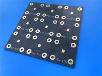
AGC Taconic TLX-6 PTFE Fiberglass Laminate PCB 2-layer 3.5mil ENIG Finish
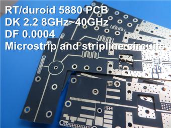
This is a type of double sided RF PCB built on RT/duroid 5880 for the application of Radar Systems.
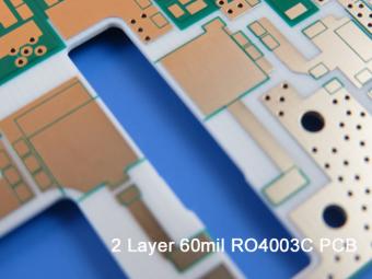
RO4003C PCBs are hydrocarbon ceramic filled laminates, not PTFE which are designed to offer superior high frequency performance.
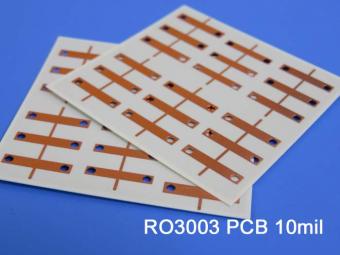
Rogers RO3003 high frequency circuit materials are ceramic-filled PTFE composites intended for use in commercial microwave and RF applications. It was designed to offer exceptional electrical and mechanical stability at competitive prices.
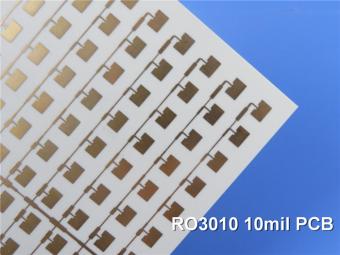
RO3010 laminates are competitively priced products with exceptional mechanical and electrical stability. This stability simplifies the design of broadband components and allows the materials to be used in a wide range of applications over a very broad range of frequencies.
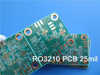
These RO3210 materials are engineered to offer exceptional electrical performance and mechanical stability. RO3210 laminates combine the surface smoothness of a non-woven PTFE laminate.
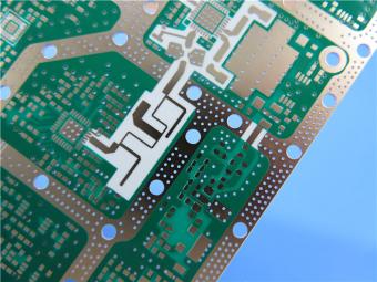
RT/duroid 6035HTC laminates are an exceptional choice for high power applications.
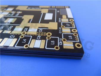
TC350 is designed to provide enhanced heat-transfer through “Best-In-Class” thermal conductivity, while reducing dielectric loss and insertion loss. Lower losses result in higher Amplifier and Antenna Gains/Efficiencies.
RO3035 materials exhibit a coefficient of thermal expansion(CTE) in the X and Y axis of 17 ppm/℃. This expansion coefficient is matched to that of copper, which allows the material to exhibit excellent dimensional stability.
 6-11C Shidai Jingyuan, Fuyong, Baoan, Shenzhen, Guangdong, China 518103


For inquiries about our products or pricelist, please leave to us and we will be in touch within 24 hours.
© Copyright: 2026 Shenzhen Bicheng Electronics Technology Co., Ltd.. All Rights Reserved.

IPv6 network supported


