

 Call Us Now !
Tel : +86 755 27374946
Call Us Now !
Tel : +86 755 27374946
 Order Online Now !
Email : info@bichengpcb.com
Order Online Now !
Email : info@bichengpcb.com
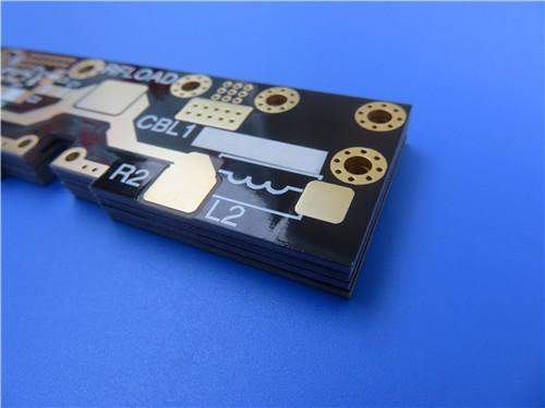
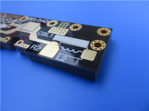
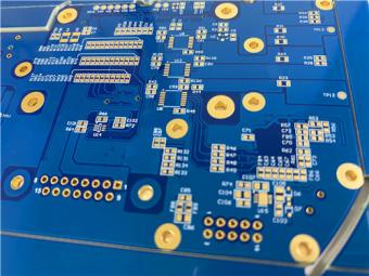
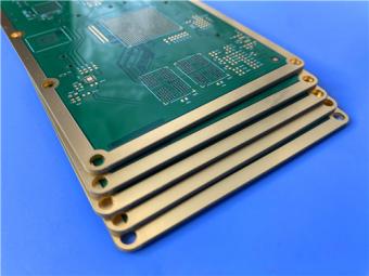
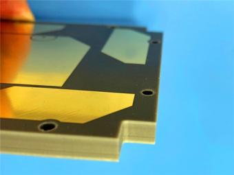
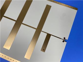
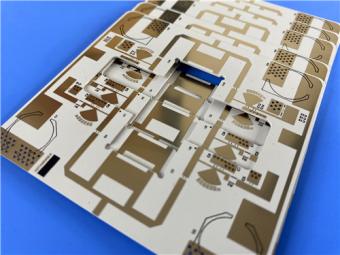
This custom double-sided high-frequency PCB integrates Wangling’s mature nano-ceramic PTFE substrate, precise 6/9mil fine line fabrication, reliable 20μm via plating, single-sided black solder mask and immersion gold surface treatment under IPC-Class-2 manufacturing standards.
Item NO.:
BIC-599-v684.0Order(MOQ):
1-10Payment:
T/TProduct Origin:
ChinaShipping Port:
ShenzhenLead Time:
7-10 days
F4BTM298 PCB 10mil Wangling Laminate 2-Layer Immersion Gold Black Solder Mask
Executive Summary
This presentation delivers an in-depth, data-backed technical introduction to the custom double-sided high-frequency PCB fabricated on Wangling F4BTM298 nano-ceramic filled PTFE CCL with 10mil core dielectric thickness, finished with electroless nickel immersion gold (Immersion Gold) surface treatment. Separated into two independent core modules—PCB Finished Board Specification and F4BTM298 Base CCL Laminate Knowledge—this article avoids data duplication, uses structured tabular technical data, highlights differentiated RF performance advantages, adheres strictly to IPC-Class-2 quality standards, and supports microwave, radar, satellite communication and phased array antenna industrial applications. All dimensional, electrical and thermal parameters are extracted from officialWangling laminate datasheets and customer fabrication specifications without exaggerated marketing claims, with clear structural logic, segmented product knowledge, and independent concluding remarks for the PCB finished board and base copper-clad laminate sections respectively.
Part 1: F4BTM298 2L Immersion Gold Finished PCB Comprehensive Introduction
1.1 Overview of PCB Construction Parameter Set
This section summarizes all dimensional, surface treatment, process and inspection specifications of the finished PCB, with key parameters organized in a standardized table for fast engineering review.
|
Parameter |
Specification |
|
Base Material |
F4BTM298 (Wangling) |
|
Layer Count |
2-layer |
|
Board Dimensions |
109 mm × 54.5 mm, ± 0.15 mm |
|
Minimum Trace/Space |
6/9 mils |
|
Minimum Hole Size |
0.4 mm |
|
Blind Vias |
Not supported |
|
Finished Board Thickness |
0.30 mm ± 0.15 mm |
|
Finished Copper Weight |
1 oz (35 μm / 1.4 mils) outer layers |
|
Via Plating Thickness |
20 μm |
|
Surface Finish |
Immersion Gold (ENIG) |
|
Top Silkscreen |
White |
|
Bottom Silkscreen |
None |
|
Top Solder Mask |
Black |
|
Bottom Solder Mask |
None |
|
Electrical Test |
100% prior to shipment |
|
Artwork Format |
Gerber RS-274-X |
|
Quality Standard |
IPC-Class-2 |
1.2 2-Layer PCB Internal Stackup Structural Breakdown
The table below illustrates the layer-by-layer stacking sequence of the 0.3mm finished PCB, centered on a10mil F4BTM298 dielectric core as the high-frequency signal transmission medium.
|
Layer |
Material |
Thickness |
|
Copper Layer 1 |
ED Copper Foil |
35 μm |
|
Dielectric Core |
F4BTM298 (PTFE + glass cloth + nano-ceramic) |
0.254 mm (10 mils) |
|
Copper Layer 2 |
ED Copper Foil |
35 μm |
1.3 PCB Circuit Statistics & Layout Component Metrics
This table quantifies all circuit layout feature counts of the finished PCB, providing clear data reference for assembly and fixture design.
|
Parameter |
Value |
|
Components |
26 |
|
Total Pads |
87 |
|
Through-Hole Pads |
49 |
|
Top SMT Pads |
38 |
|
Bottom SMT Pads |
0 |
|
Vias |
31 |
|
Nets |
2 |
1.4 Core Differentiated Performance Advantages of This F4BTM298 RF PCB
Unlike conventional FR4, low-grade PTFE or ceramic-filled hydrocarbon PCBs, this2-layer Immersion GoldWanglingPCB delivers targeted advantages for microwave engineering:
1) Ultra-Stable High-Frequency Dielectric Performance:
Built on F4BTM298 CCL with Dk=2.98±0.06 and Df=0.0018 at 10GHz, the 10mil thin core minimizes signal propagation delay while maintaining ultra-low insertion loss, critical for phase shifters and phased array feed networks.
2) Optimized Single-Sided Mask & Silkscreen Design:
Removing bottom solder mask eliminates extra dielectric coating above the ground plane, reducing parasitic capacitance and improving RF isolation between signal traces and ground copper. White top silkscreen ensures clear component marking without interfering with top-side high-frequency traces.
3) Immersion Gold Flat Surface for Precision SMT:
The electroless nickel-gold finish delivers uniform planar surface compared to HASL tin-lead, supporting the board’s 38 top SMT pads with consistent solder wetting, avoiding cold joints common in RF passive component assembly. The 20μm via plating thickness reinforces hole wall reliability under repeated thermal cycling of radar and base station equipment.
4) Low Thermal Expansion Matching for Long-Term Stability:
Supported by the base laminate’s X/Y CTE of 15/16 ppm/°C, the PCB resists line cracking and pad lifting under -55°C to 288°C operating temperature range, a core advantage over organic high-frequency substrates with high thermal expansion.
1.5 Typical Application Scenarios for This Finished PCB
This thin 10mil 2-layer F4BTM298 Immersion Gold PCB is engineered for compact, lightweight high-frequency RF modules without strict PIM requirements, including microwave radar front-end circuits, miniaturized phase shifters, micro power dividers, RF couplers, satellite communication receive feed networks, compact base station antenna matching circuits, and small phased array antenna unit boards.
The thin 10mil core reduces overall module thickness for portable RF testing equipment and airborne communication payloads.
1.6 Conclusion for Finished F4BTM298 2L Immersion Gold PCB
This custom double-sided high-frequency PCB integrates Wangling’s mature nano-ceramic PTFE substrate, precise 6/9mil fine line fabrication, reliable 20μm via plating, single-sided black solder mask and immersion gold surface treatment under IPC-Class-2 manufacturing standards. All dimensional, electrical and structural parameters are strictly controlled within published tolerance ranges, with differentiated design optimizations targeting low microwave loss, stable impedance and long-term thermal cycling reliability. The simple two-net circuit layout balances production cost and RF performance, making it a cost-effective standardized solution for mass production of non-PIM sensitive microwave and satellite communication hardware, with full global delivery support and complete pre-shipment quality verification to reduce end-user assembly failure risks.
Part 2: Deep Dive into F4BTM298 Base Copper-Clad Laminate (CCL)
2.1 CCL Product Foundation & Raw Material Composition
F4BTM298 is a proprietary nano-ceramic filled PTFE fiberglass copper-clad laminate manufactured by Wangling Insulation Material Factory, formulated with woven fiberglass cloth, high-dielectric low-loss nano-ceramic powder and pure PTFE resin, then pressed under high-temperature high-pressure standardized lamination processes. The material upgrades the base F4BM PTFE dielectric platform by adding nano-ceramic fillers, delivering elevated dielectric constant, improved heat resistance, reduced thermal expansion coefficient, higher insulation resistance and enhanced thermal conductivity while retaining the intrinsic ultra-low dissipation factor of PTFE substrates.
Two variant grades share identical dielectric core but differ in copper foil matching:
- F4BTM298: Matched with standard ED electro-deposited copper foil, designed for applications without passive intermodulation (PIM) performance demands, the exact CCL used for this finished PCB.
- F4BTME298: Matched with reverse-treated RTF copper foil, offering superior≤-160dBc PIM performance, finer line control and lower conductor loss for carrier-grade base station antennas.
2.2 Full Official Datasheet Parameter Table of F4BTM298 Laminate
Table 4: F4BTM298 CCL Complete Technical Datasheet
|
Performance Item |
Test Condition |
Unit |
F4BTM298 Standard Value |
|
Dielectric Constant (Dk) |
10GHz, Z-axis |
/ |
2.98 ± 0.06 |
|
Dissipation Factor (Df) |
10GHz |
/ |
0.0018 |
|
Dissipation Factor (Df) |
20GHz |
/ |
0.0023 |
|
Dk Temperature Coefficient |
-55℃ ~ 150℃ |
ppm/℃ |
-78 |
|
X-axis CTE |
-55℃ ~ 288℃ |
ppm/℃ |
15 |
|
Y-axis CTE |
-55℃ ~ 288℃ |
ppm/℃ |
16 |
|
Z-axis CTE |
-55℃ ~ 288℃ |
ppm/℃ |
78 |
|
Peel Strength (1oz ED copper) |
Room Temp |
N/mm |
>1.6 |
|
Volume Resistivity |
Normal Condition |
MΩ·cm |
≥1×10⁷ |
|
Surface Resistance |
Normal Condition |
MΩ |
≥1×10⁶ |
|
Z-direction Dielectric Strength |
5KV, 500V/s |
KV/mm |
>26 |
|
XY-direction Breakdown Voltage |
5KV, 500V/s |
KV |
>34 |
|
Water Absorption |
20±2℃, 24h |
% |
≤0.05 |
|
Density |
Ambient Temp |
g/cm³ |
2.25 |
|
Continuous Operating Temp |
Constant Operation |
℃ |
-55 ~ +260 |
|
Z-direction Thermal Conductivity |
Standard Test |
W/(M·K) |
0.42 |
|
Flammability Standard |
UL Certification |
Grade |
UL-94 V0 |
|
Thermal Stress Resistance |
260℃, 10s, 3 cycles |
Result |
No Delamination |
|
PIM Index |
F4BTME298 Only |
dBc |
≤-160 |
|
Core Material Composition |
- |
- |
PTFE resin + fiberglass cloth + nano-ceramic filler |
2.3 CCL Customization & Supply Specifications
1) Copper Foil Thickness Options for F4BTM Series:
ED copper foil available in 0.5OZ (0.018mm), 1OZ (0.035mm), 1.5OZ (0.05mm), 2OZ (0.07mm), fully matching the 1oz outer copper specification of the finished PCB.
2) Standard Panel Sizes
|
Panel Size (mm) |
Availability |
|
460 × 610 |
Standard |
|
600 × 500 |
Standard |
|
914 × 1220 |
Standard (for thickness < 4.0 mm) |
3) Standard Thickness Options–Total Copper Thickness or Dielectric Thickness (Customer Specifies)
|
Thickness (mm) |
Tolerance (mm) |
|
0.254 (minimum) |
±0.02 |
|
0.508 |
±0.04 |
|
0.762 |
±0.05 |
|
0.8 |
±0.05 |
|
1 |
±0.05 |
|
1.016 |
±0.05 |
|
1.27 |
±0.06 |
|
1.524 |
±0.06 |
|
2 |
±0.075 |
|
3 |
±0.09 |
|
4 |
±0.10 |
|
5 |
±0.10 |
|
6 |
±0.12 |
|
8 |
±0.15 |
|
10 |
±0.18 |
|
12 |
±0.20 |
Note: This specific PCB uses a 0.254 mm dielectric core (10 mils) with 35μm copper on both sides.
4) Metal-Backed Derivative Substrates:
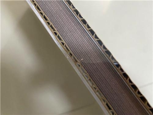
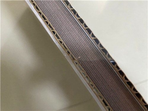
Custom aluminum base (F4BTM298-AL) or copper base (F4BTM298-CU) variants are available for enhanced heat dissipation and electromagnetic shielding, applicable to high-power RF amplifier modules.
5). Metal-Backed Derivative Substrates:
Custom aluminum base (F4BTM298-AL) or copper base (F4BTM298-CU) variants are available for enhanced heat dissipation and electromagnetic shielding, applicable to high-power RF amplifier modules.
2.4 Unique Material Differentiation of F4BTM298 CCL vs Conventional RF Substrates
1)Nano-Ceramic Filler Optimization: Compared to traditional pure PTFE fiberglass substrates without ceramic doping, the nano-ceramic filler lowers overall thermal expansion coefficient and elevates thermal conductivity, mitigating heat accumulation in long-running RF power circuits.
2) Ultra-Low Moisture Absorption (≤0.05%): Minimal water uptake avoids Dk shift under humid field environments, stabilizing antenna gain and phase consistency for outdoor base station and satellite equipment.
3) Wide Temperature Dk Stability: Dk temperature coefficient of -78 ppm/℃from -55℃to 150℃delivers consistent signal impedance across extreme cold and high-temperature working conditions, superior to hydrocarbon and low-end ceramic-filled RF laminates with large Dk drift.
4) Flame Retardant UL-94 V0 Rating: Self-extinguishing property meets industrial communication equipment safety standards, eliminating fire risks from high-power RF component heat generation.
5) Radiation Resistance & Low Outgassing: Suitable for aerospace satellite communication payloads operating in vacuum space environments, a critical advantage over non-PTFE high-frequency substrates.
2.5 Conclusion for F4BTM298 Base Copper-Clad Laminate
F4BTM298 is a cost-effective, mass-producible nano-ceramic modified PTFE high-frequency CCL tailored for non-PIM RF and microwave systems, balancing ultra-low high-frequency loss, stable dielectric constant, excellent thermal mechanical performance and industrial scalability. The standardized 10mil thin core variant selected for the finished 2-layer Wangling F4B DK2.98 PCB achieves compact board thickness while maintaining complete RF signal integrity. With customizable copper foil thickness, panel sizes and metal-backed derivative versions, this laminate supports diversified RF product development from miniaturized radar modules to large phased array antenna feed boards.
All electrical, thermal and mechanical performance data comply with IPC-TM650 and GB/T 12636-1990 test standards, providing reliable, repeatable substrate performance for consistent PCB batch fabrication, and serves as the core foundational material enabling the finished PCB’s targeted low-loss microwave operating characteristics.
Previous:
Wangling WL-CT350 4mil Laminate PCB 2-Layer Immersion Gold No Solder Mask Black SilkscreenNext:
Wangling 5mil 0.127mm TFA300 Core 2-layer Immersion Gold Green Solder Mask PCBIf you have questions or suggestions,please leave us a message,we will reply you as soon as we can!
Categories
New Products
8-Layer Hybrid RF PCB: RO4350B + TG170 FR-4 + RO4003C with RO4450F Bondply
4-Layer Rogers RO3010 Hybrid PCB Immersion Silver 2.8mm Finished Thickness
4-Layer 20mil Rogers RO3210 ISIG High-Frequency PCB with Controlled Depth Milling
4-Layer 10mil RO3003 + Tg170 FR-4 Hybrid PCB with ENIG and Controlled Depth Milling
2-Layer F4BM233 4.0mm Wangling Substrate High-Frequency Custom PCB with ENIG Finish
Wangling WL-CT615 8mil Ultra-Thin High-Frequency 2-Layer PCB ENEPIG Finish
High-Frequency 2-Layer PCB on 59mil Wangling TP440 Thermoplastic Dielectric Immersion Gold
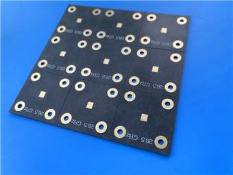
AGC Taconic TLX-6 PTFE Fiberglass Laminate PCB 2-layer 3.5mil ENIG Finish

RF-10 25mil Taconic PCB Materials stands out as a high-performance solution for RF applications. Its exceptional electrical properties, dimensional stability, thermal conductivity, and adhesion characteristics make it an ideal choice for demanding applications.
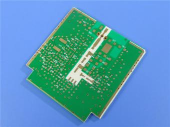
The PCB has a 4-layer hybrid stackup with a 0.5oz+plating ground layer, two 1oz ground layers, and a 0.5oz+plating signal layer.
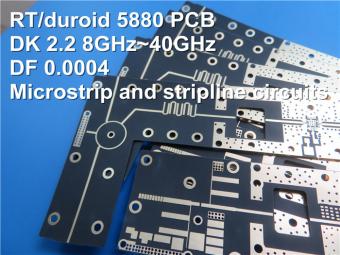
The dimensions of the board are 55.00 x 26.00 mm, with a tolerance of +/- 0.15mm. The board has 16 components, 26 total pads, 9 through-hole pads, 10 top SMT pads, 7 bottom SMT pads, 77 vias, and 82 nets.
Rogers RO4003C PCB is an innovative and advanced circuit board that is made with high-quality materials.
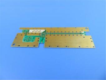
The RO4350B PCB offers a range of benefits that make it an ideal choice for high-frequency applications. Its low dielectric loss and high thermal conductivity make it perfect for high-frequency applications such as RF and microwave circuits.

Bicheng PCB Ships High-Quality PCBs with Shengyi Tg150 ℃ S1000H Material and Advanced Stackup
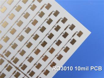
Rogers RO3010 PCB is ideal for a wide range of high-frequency applications, including power amplifiers, filters, couplers, and antennas.
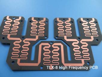
TLX-8 features low dielectric loss, low moisture absorption, and excellent thermal stability, making it ideal for high-frequency and high-speed applications. It has a low dissipation factor, which helps to minimize signal loss and distortion.
 6-11C Shidai Jingyuan, Fuyong, Baoan, Shenzhen, Guangdong, China 518103


For inquiries about our products or pricelist, please leave to us and we will be in touch within 24 hours.
© Copyright: 2026 Shenzhen Bicheng Electronics Technology Co., Ltd.. All Rights Reserved.

IPv6 network supported


