

 Call Us Now !
Tel : +86 755 27374946
Call Us Now !
Tel : +86 755 27374946
 Order Online Now !
Email : info@bichengpcb.com
Order Online Now !
Email : info@bichengpcb.com
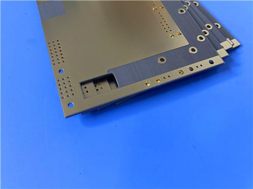
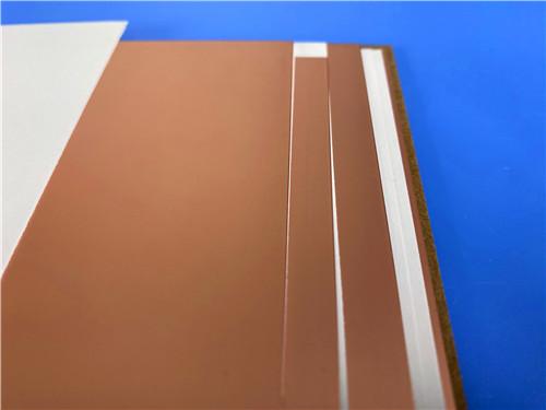
This 2-layer F4BM255 3.0mm laminate PCB is a cost-effective, high-performance microwave circuit solution balancing low dielectric loss, dimensional stability and heavy-current transmission capacity.
Item NO.:
BIC-604-v689.0Order(MOQ):
1-10Payment:
T/TProduct Origin:
ChinaShipping Port:
ShenzhenLead Time:
7-10 days
Wangling 2-Layer F4BM255 3.0mm DK2.55 Substrate 2oz Heavy Copper ENIG PCB
Part 1: PCB Product Core Introduction
1.1 Product Overview
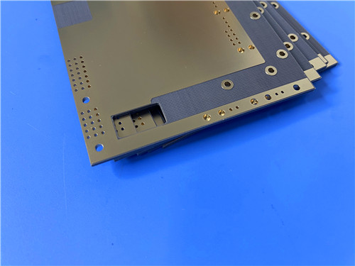
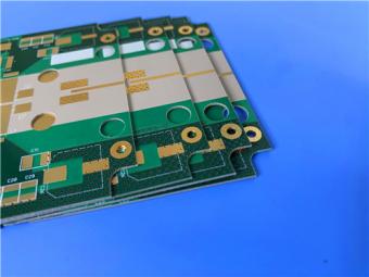
This custom two-layer rigid RF/microwave printed circuit board is built on Taizhou Wangling Insulation Factory’s F4BM255 PTFE glass fabric copper-clad laminate (CCL), with a full dielectric core thickness of 3.0mm, targeted for medium-to-high frequency RF circuits without strict Passive Intermodulation (PIM) requirements. The finished board dimension is 521mm×59mm (1 piece only), adopting 2oz heavy copper outer layers, immersion gold surface finish, single-sided green solder mask and single-sided white silkscreen.
F4BM255 substrate is engineered to balance low high-frequency dielectric loss and dimensional stability, outperforming traditional F4B series PTFE laminates with tighter DK tolerance, elevated insulation resistance and consistent electrical performance across -55°C to +260°C operating temperature range. This 2-layer Wangling PCB design eliminates blind/buried vias and relies purely on through-hole interconnection, simplifying fabrication while preserving critical signal integrity for microwave passive components, short-range radar feed networks and medium-power RF antenna assemblies. The 2oz thick copper construction reduces conductor loss under continuous RF power loading, while immersion gold surface finish delivers excellent oxidation resistance, stable contact impedance for SMT component soldering and long-term storage durability without black pad defects.
1.2 PCB Construction Details
Full mechanical, material and surface finishing specifications of the2-layer F4BM255 PCB
|
Parameter |
Specification |
|
Base Material |
F4BM255 (PTFE + Woven Fiberglass) |
|
Layer Count |
2-layer rigid |
|
Board Dimensions |
521mm × 59mm (±0.15mm), 1 piece per panel |
|
Finished Board Thickness |
3.1mm (3.0mm dielectric + 2×70μm copper) |
|
Minimum Trace/Space |
7/7 mils |
|
Minimum Hole Size |
0.4mm |
|
Blind/Buried Vias |
None |
|
Finished Copper Weight |
2 oz (70μm) on outer layers |
|
Via Plating Thickness |
20μm |
|
Surface Finish |
Immersion Gold (ENIG) |
|
Top Solder Mask |
Green |
|
Bottom Solder Mask |
None |
|
Top Silkscreen |
White |
|
Bottom Silkscreen |
None |
|
Electrical Test |
100% prior to shipment |
|
Artwork Format |
Gerber RS-274-X |
|
Quality Standard |
IPC-Class-2 |
|
Availability |
Worldwide |
1.3 PCB Stackup Structure
This two-layer stackup adopts symmetrical single-core PTFE structure without prepreg interlayers, featuring uniform heavy copper cladding on both sides of thick F4BM dielectric core.
|
Layer |
Material |
Thickness |
|
Layer 1 (Top) |
Copper |
70μm (2 oz) |
|
Core |
F4BM255 Dielectric |
3.0mm |
|
Layer 2 (Bottom) |
Copper |
70μm (2 oz) |
1.4 PCB Circuit Statistical Data
Quantitative circuit metrics including pads, vias, nets and component count for design reference
|
Parameter |
Value |
|
Components |
28 |
|
Total Pads |
194 |
|
Through-Hole Pads |
148 |
|
Top SMT Pads |
46 |
|
Bottom SMT Pads |
0 |
|
Vias |
43 |
|
Nets |
2 |
1.5 Manufacturing & Application Differentiation Advantages
1) Low-loss high-frequency substrate advantage: F4BM255 delivers DF = 0.0013 @10GHz, drastically reducing signal attenuation for microwave frequency bands from 2GHz to 20GHz;2)tighter DK tolerance±0.05 ensures consistent impedance matching across full panel length of 521mm.
3) 2oz heavy copper performance: Thick copper layer minimizes skin-effect conductor loss under continuous RF power, suitable for power divider, coupler and medium-power antenna feed circuits where high current throughput is required.
4) Controlled thermal mechanical stability: F4BM255 XY-axis CTE only 16–21 ppm/°C, preventing trace cracking during reflow (260°C peak temperature) and long-term cyclic temperature variation from -55°C to 260°C.
5) Cost-optimized single-sided coating scheme: Eliminating bottom solder mask and silkscreen cuts raw material and coating labor cost while retaining full trace protection on the signal-carrying top surface.
6) Large-format customized capability: Supports non-standard long strip dimension 521mm×59mm, compatible with linear antenna arrays, series-connected passive RF module assemblies that require extended PCB length.
1.6 PCB Conclusion
This 2-layer F4BM255 3.0mm laminate PCB is a cost-effective, high-performance microwave circuit solution balancing low dielectric loss, dimensional stability and heavy-current transmission capacity. Its standardized fabrication rules (IPC-Class-2), worldwide production compatibility via Gerber RS-274-X artwork, and flexible customized dimension capability make it a mature substitute for imported foreign PTFE RF PCBs for non-PIM sensitive RF passive and antenna systems. The simplified through-hole-only stackup reduces manufacturing difficulty and lead time, while the single-sided green mask + white silkscreen layout achieves optimal balance between functional protection and project cost control, covering mainstream commercial microwave communication application scenarios.
Part 2: Supporting CCL Deep Technical Explanation–F4BM255 PTFE Glass Fabric Copper Clad Laminate
2.1 CCL Product Definition & Raw Material Formulation
F4BM255 is a PTFE woven glass fabric reinforced copper-clad laminate manufactured by Taizhou Wangling Insulation Material Factory, compounded by high-purity polytetrafluoroethylene resin, PTFE film and E-glass woven cloth under precise temperature & pressure lamination molding process. Compared to the base F4B series PTFE substrates, F4BM series upgrades formula uniformity to expand DK adjustable range, lower dissipation factor and raise volume/surface insulation resistance with superior batch-to-batch consistency.
Core classification difference between F4BM and F4BME: identical PTFE-glass dielectric core, differentiated only by attached copper foil type. F4BM series uses standard ED (electrodeposited) copper foil without optimized reverse roughness structure, making it ideal for applications without mandatory PIM performance indicators; F4BME adopts reverse-treated RTF copper foil for ultra-low PIM≤-159 dBc, targeting carrier-grade base station antennas. F4BM255’s 2.55 DK value is tuned by adjusting glass fiber proportion inside PTFE matrix: higher glass loading improves XY dimensional stability, lowers thermal expansion coefficient and temperature drift, with minor trade-off of slightly elevated dielectric loss versus lower-DK pure PTFE substrates.
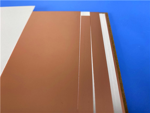
2.2 Full F4BM255 Datasheet Technical Parameter Table
(Summary: Complete electrical, thermal, mechanical and environmental performance metrics under standardized test conditions)
|
Performance Item |
Test Condition |
Unit |
F4BM255 Standard Value |
|
Nominal Dielectric Constant (DK) |
10 GHz |
/ |
2.55 |
|
DK Tolerance |
N/A |
/ |
±0.05 |
|
Dissipation Factor (DF, Loss Tangent) |
10 GHz |
/ |
0.0013 |
|
Dissipation Factor (DF, Loss Tangent) |
20 GHz |
/ |
0.0018 |
|
DK Temperature Coefficient |
-55°C ~ +150°C |
ppm/°C |
-110 |
|
Peel Strength (1oz ED Copper) |
Room temp |
N/mm |
>1.8 |
|
Volume Resistivity |
Ambient normal state |
MΩ·cm |
≥6×10⁶ |
|
Surface Resistivity |
Ambient normal state |
MΩ |
≥1×10⁶ |
|
Z-Axis Dielectric Strength |
5kV, 500V/s ramp |
kV/mm |
>25 |
|
XY-Axis Breakdown Voltage |
5kV, 500V/s ramp |
kV |
>34 |
|
XY Thermal Expansion Coefficient (CTE) |
-55°C ~ 288°C |
ppm/°C |
16 ~ 21 |
|
Z Thermal Expansion Coefficient (CTE) |
-55°C ~ 288°C |
ppm/°C |
173 |
|
Thermal Stress Resistance |
260°C immersion, 10s, 3 cycles |
Qualitative |
No delamination, no blistering |
|
Water Absorption Rate |
20±2°C, 24h soak |
% |
≤0.08 |
|
Material Density |
Room temperature |
g/cm³ |
2.25 |
|
Continuous Operating Temperature Range |
Thermal cycling chamber |
°C |
-55 ~ +260 |
|
Z-Axis Thermal Conductivity |
Ambient |
W/(m·K) |
0.33 |
|
PIM Index |
Only valid for F4BME series |
dBc |
N/A (F4BM no PIM optimization) |
|
Flammability Rating |
UL standard test |
Grade |
UL-94 V-0 |
|
Core Material Composition |
N/A |
/ |
PTFE resin + woven glass fabric, cladded with ED copper foil |
2.3 Optional Copper Foil, Dimension & Thickness Customization Specifications
2.3.1 Copper Foil Options for F4BM Series
This PCB project selects 2oz ED copper matching the high-current circuit design requirement.
2.3.2 Standard & Customizable Panel Sizes
2.3.3 Standard Dielectric Thickness & Tolerance Chart
Available core dielectric thickness covers 0.1mm minimum (DK≤2.65) up to 12.0mm thick substrate, with graded dimensional tolerances based on thickness:
Ultra-thin (<0.1mm) or extra-thick (>12mm) dielectric layers support customized development via factory special pressing process.
2.4 Optional Derivative Products: F4BM255 Metal-Base Substrates
F4BM255 can be laminated with aluminum base or copper base to form heat-dissipating shielded metal-clad CCL, model naming rule:
Metal base thickness options: 0.48mm, 0.98mm, 1.48mm, 1.98mm, 2.98mm, 3.98mm, tolerance +0.02/-0.05mm. Metal-base laminates are used for high-power RF modules requiring passive heat sinking and electromagnetic shielding integration.
2.5 Core Product Characteristics of F4BM255 CCL
1)Wide adjustable DK spectrum (2.17~3.0 customizable), fixed nominal DK 2.55 for this series grade with tight±0.05 tolerance for stable impedance control.
2)Ultra-low high-frequency dielectric loss, maintaining DF below 0.002 across 10–20GHz frequency band, critical for long-distance signal transmission in antenna feed networks.
3)Glass-reinforced matrix delivers excellent dimensional stability and low XY CTE, preventing PCB warpage and trace fracture under wide temperature fluctuation.
4)Multi-size panel & multi-thickness dielectric customization capability, reduces material waste for long-strip PCB designs like the 521mm-length product.
5)Radiation-resistant and low outgassing performance, compliant with aerospace and satellite communication component material requirements.
6)Mass industrialized production with cost competitiveness, serves as domestic replacement solution for imported foreign PTFE microwave laminates.
2.6 Typical Industrial Application Fields for F4BM255 CCL
All circuits fabricated on F4BM255 substrate fit RF/microwave systems without strict PIM testing standards:
2.7 CCL Material Conclusion
F4BM255 PTFE glass fabric copper-clad laminate is a balanced-performance high-frequency substrate optimized for cost-sensitive commercial microwave electronics. Its precisely controlled 2.55 dielectric constant, ultra-low dissipation factor, reinforced glass matrix thermal stability and full customization of thickness, panel size and copper foil weight make it the ideal base material for the 2-layer 3.0mm thick RF PCB described above. Distinguished from low-PIM F4BME variant by standard ED copper foil configuration, F4BM255 eliminates unnecessary reverse copper surface processing cost while retaining core low-loss dielectric performance, positioning it as the preferred substrate for non-PIM critical RF antenna, radar and passive component manufacturing with stable domestic supply chain and import substitution value.
Previous:
2-layer Isola I-Tera MT40 10mil Core PCB With Immersion SilverNext:
Wangling WL-CT350 4mil Laminate PCB 2-Layer Immersion Gold No Solder Mask Black SilkscreenIf you have questions or suggestions,please leave us a message,we will reply you as soon as we can!
Categories
New Products
Wangling F4BTMS220 2-Layer DK2.2 PCB 10 mil Core with Immersion Gold
Wangling F4BTME350 10mil DK3.5 High Frequency Substrate PCB 2-Layer Immersion Gold
Wangling F4BTM300 Custom 2-layer PCB 20mil DK3.0 Substrate with Immersion Gold
Rogers 20mil RT/duroid 6202 2-layer ENIG High-Frequency Microwave PCB
Rogers 20mil AD250C PCB Pure Gold High-Frequency Antenna Circuit Board
8-Layer Hybrid RF PCB: RO4350B + TG170 FR-4 + RO4003C with RO4450F Bondply
4-Layer Rogers RO3010 Hybrid PCB Immersion Silver 2.8mm Finished Thickness
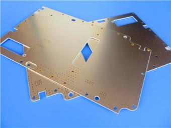
4-Layer 20mil Rogers RO3210 ISIG High-Frequency PCB with Controlled Depth Milling

RF-10 25mil Taconic PCB Materials stands out as a high-performance solution for RF applications. Its exceptional electrical properties, dimensional stability, thermal conductivity, and adhesion characteristics make it an ideal choice for demanding applications.
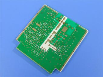
The PCB has a 4-layer hybrid stackup with a 0.5oz+plating ground layer, two 1oz ground layers, and a 0.5oz+plating signal layer.
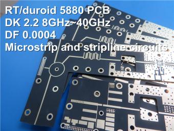
The dimensions of the board are 55.00 x 26.00 mm, with a tolerance of +/- 0.15mm. The board has 16 components, 26 total pads, 9 through-hole pads, 10 top SMT pads, 7 bottom SMT pads, 77 vias, and 82 nets.
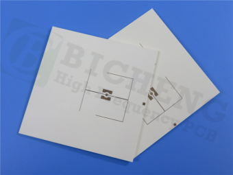
Rogers RO4003C PCB is an innovative and advanced circuit board that is made with high-quality materials.
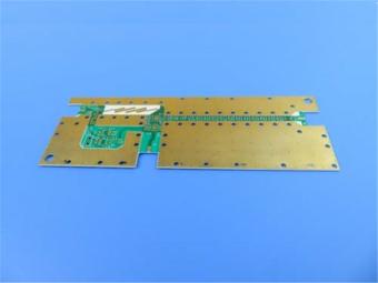
The RO4350B PCB offers a range of benefits that make it an ideal choice for high-frequency applications. Its low dielectric loss and high thermal conductivity make it perfect for high-frequency applications such as RF and microwave circuits.

Bicheng PCB Ships High-Quality PCBs with Shengyi Tg150 ℃ S1000H Material and Advanced Stackup
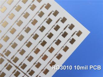
Rogers RO3010 PCB is ideal for a wide range of high-frequency applications, including power amplifiers, filters, couplers, and antennas.
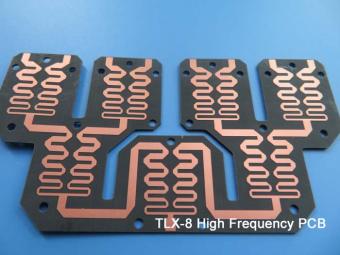
TLX-8 features low dielectric loss, low moisture absorption, and excellent thermal stability, making it ideal for high-frequency and high-speed applications. It has a low dissipation factor, which helps to minimize signal loss and distortion.
 6-11C Shidai Jingyuan, Fuyong, Baoan, Shenzhen, Guangdong, China 518103


For inquiries about our products or pricelist, please leave to us and we will be in touch within 24 hours.
© Copyright: 2026 Shenzhen Bicheng Electronics Technology Co., Ltd.. All Rights Reserved.

IPv6 network supported


