

 Call Us Now !
Tel : +86 755 27374946
Call Us Now !
Tel : +86 755 27374946
 Order Online Now !
Email : info@bichengpcb.com
Order Online Now !
Email : info@bichengpcb.com
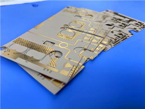
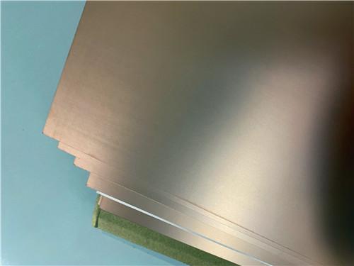
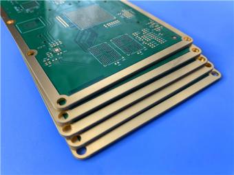
This immersion gold WL-CT350 RF PCB forms a cost-performance balanced high-frequency circuit solution that bridges the performance gap between low-loss PTFE laminates and low-cost FR4 materials.
Item NO.:
BIC-603-v688.0Order(MOQ):
1-10Payment:
T/TProduct Origin:
ChinaShipping Port:
ShenzhenLead Time:
7-10 days
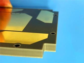
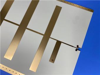
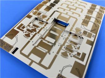
Wangling WL-CT350 4mil Laminate PCB 2-Layer Immersion Gold No Solder Mask Black Silkscreen
Executive Summary
This presentation delivers an in-depth, data-backed technical overview of the 2-layer WL-CT350 hydrocarbon ceramic RF PCB finished with immersion gold surface treatment, separated into two independent modules: finished PCB assembly specifications and underlyingWL-CT350 copper clad laminate(CCL) core material analysis. The Wangling PCB targets microwave, aerospace, radar and satellite communication scenarios, balancing FR4-compatible manufacturability, stable high-frequency electrical performance, low passive intermodulation (PIM), and wide-temperature mechanical reliability—an economical alternative to traditional PTFE-based RF substrates likeTaconic TLX-8 without complex specialized fabrication workflows.
All dimensional, electrical and thermal parameters strictly follow IPC-Class-2 acceptance criteria, with full 100% electrical continuity testing before shipment. Distinct competitive differentiators include thermosetting hydrocarbon-ceramic dielectric architecture, ultra-low Z-axis CTE, Tg exceeding 280°C, and consistent Dk/Df stability across 0.5–25 GHz frequency bands, paired with immersion gold finish that optimizes SMT solderability and minimizes signal loss for precision RF circuits.
Part 1: WL-CT350 2L Immersion Gold PCB Finished Board Specification
1.1 PCB Construction Details Overview
This table aggregates all mechanical, manufacturing, surface finish and quality inspection specifications of the finished 2-layer RF PCB.
|
Parameter |
Specification |
|
Layer Count |
2-layer |
|
Base Material |
WL-CT350 |
|
Board Dimensions |
56.8 mm × 78.09 mm per panel, ±0.15 mm |
|
Minimum Trace/Space |
6 / 7 mils (0.152 / 0.178 mm) |
|
Minimum Hole Size |
0.3 mm (mechanical drilled, no blind vias) |
|
Finished Board Thickness |
0.2 mm (±10% tolerance typical) |
|
Finished Copper Weight |
1 oz (35 µm / 1.4 mils) outer layers |
|
Via Plating Thickness |
20 µm (minimum) |
|
Surface Finish |
Immersion Gold (ENIG) |
|
Top Silkscreen |
Black |
|
Bottom Silkscreen |
No |
|
Top Solder Mask |
No |
|
Bottom Solder Mask |
No |
|
Electrical Test |
100% flying-probe or fixture testing prior to shipment |
|
Artwork Format |
Gerber RS-274-X |
|
Acceptance Standard |
IPC-Class-2 |
1.2 PCB Stackup Architecture Overview
This simplified table defines the symmetrical two-layer core stackup of the rigid PCB, using standard WL-CT350 4mil dielectric core with double-sided 35μm copper cladding.
|
Layer |
Material |
Thickness |
|
Copper Layer 1 (Top) |
ED copper foil |
35 µm (1 oz) |
|
Dielectric Core |
WL-CT350 (hydrocarbon-ceramic) |
0.102 mm (4 mils) |
|
Copper Layer 2 (Bottom) |
ED copper foil |
35 µm (1 oz) |
1.3 PCB Circuit Statistical Data Overview
This table quantifies circuit geometry component counts, pad types, vias and signal network layout metrics for the sample PCB design.
|
Item |
Count |
|
Components |
19 |
|
Total Pads |
32 |
|
Through Hole Pads |
18 |
|
Top SMT Pads |
14 |
|
Bottom SMT Pads |
0 |
|
Vias |
11 (all plated through-hole) |
|
Nets |
2 |
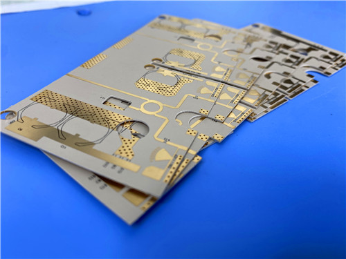
1.4 Manufacturing & Performance Differentiators of WL-CT350 2L Immersion Gold PCB
1.5 Typical Finished PCB Application Scenarios
The WL-CT350 2-layer immersion gold PCB is engineered for mid-to-high frequency RF hardware operating between 0.5 GHz and 25 GHz, including:
Its mechanical stability under severe vibration and extreme temperature fluctuations makes it suitable for space launch vibration environments and marine naval antenna hardware where PTFE alternatives incur excessive processing overhead.
1.6 Conclusion for Finished WL-CT350 PCB
This immersion gold WL-CT350 RF PCB forms a cost-performance balanced high-frequency circuit solution that bridges the performance gap between low-loss PTFE laminates and low-cost FR4 materials. Standardized FR4 manufacturability cuts fabrication complexity without sacrificing stable Dk/Df, low PIM (≤-157 dBc with RTF copper foil), wide temperature dimensional stability and UL94 V-0 flame retardancy. The solder-mask-free design, precise 20μm via plating, IPC-Class-2 quality assurance and immersion gold surface treatment collectively deliver consistent signal integrity for microwave passive and active circuits, serving as a drop-in upgrade option to replace imported PTFE PCBs for commercial and aerospace-grade RF hardware.
Part 2: In-Depth WL-CT350 CCL Copper Clad Laminate Core Material Knowledge
2.1 WL-CT350 CCL Product General Introduction
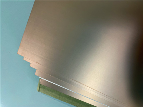
WL-CT350 belongs to the Wangling WL-CT series thermosetting organic polymer ceramic-filled woven fiberglass copper clad laminate manufactured by Taizhou Wangling Insulation Material Factory, constructed from a ternary composite system of hydrocarbon resin, micron-scale ceramic filler and E-glass woven cloth reinforcement. It differentiates itself from thermoplastic PTFE RF substrates (e.g., TLX-8 PTFE glass laminates) via cross-linked thermosetting resin chemistry, which delivers superior mechanical rigidity, higher glass transition temperature (Tg > 280°C), simplified FR4-compatible PCB processing, and controlled thermal expansion in X/Y/Z axes. The material targets microwave and aerospace applications requiring low insertion loss, minimal dielectric constant shift under temperature variation, anti-radiation performance and low vacuum outgassing compliant with space industry vacuum volatile standards.
WL-CT350 supports two copper foil variants: standard ED (Electrodeposited) copper foil and reverse-treated RTF copper foil. RTF foil features adhesive backing that boosts PIM performance down to≤-157 dBc by smoothing conductor surface roughness to reduce intermodulation distortion, ideal for passive antenna components sensitive to signal interference; ED copper foil offers higher peel strength (0.85 N/mm for 1 oz foil) for heavy-duty mechanical assembly such as bolted radar substrates. Customizable dielectric thickness ranges from 4 mil (0.102 mm) up to 60+ mil, with 30 mil (0.762 mm) core selected for the above finished PCB stackup to balance impedance control and mechanical rigidity. The laminate can also be bonded to aluminum base to form WL-CT350-AL metal-core RF substrates for high-power amplifier thermal dissipation requirements.
2.2 Full WL-CT350 CCL Datasheet Technical Parameter Table
All test standards reference IPC-TM-650, GB/T 4722-2017 and GB/T 12636-1990, with all values listed as typical measured performance data for design reference only.
|
Test Item |
Test Condition |
Unit |
WL-CT350 Standard Value |
|
Dielectric Constant (Typical Dk) |
10 GHz, Z-axis stripline |
- |
3.48 |
|
Dielectric Constant (Design Dk) |
10 GHz, 50Ω microstrip |
- |
3.66 |
|
Dk Tolerance |
Full frequency band |
- |
±0.05 |
|
Dissipation Factor Df |
2 GHz |
- |
0.003 |
|
Dissipation Factor Df |
10 GHz |
- |
0.0039 |
|
Dissipation Factor Df |
20 GHz |
- |
0.0048 |
|
TCDK (Dielectric Constant Temp Coefficient) |
-55°C ~ +150°C |
ppm/°C |
52 |
|
Peel Strength (1 oz ED Copper) |
Room temperature |
N/mm |
0.85 |
|
Peel Strength (1 oz RTF Copper) |
Room temperature |
N/mm |
0.72 |
|
Volume Resistivity |
Ambient condition |
MΩ·cm |
1×10⁹ |
|
Surface Resistivity |
Ambient condition |
MΩ |
4×10⁹ |
|
Electrical Strength (Z-axis) |
5 kV, 500 V/s ramp |
kV/mm |
31 |
|
XY Direction Breakdown Voltage |
5 kV, 500 V/s ramp |
kV |
30 |
|
X/Y Axis CTE |
-55°C ~ 288°C |
ppm/°C |
11.14 |
|
Z Axis CTE |
-55°C ~ 288°C |
ppm/°C |
34 |
|
Thermal Stress Reliability |
288°C solder float, 10s × 3 cycles |
- |
No delamination, no blister |
|
Moisture Absorption Rate |
23.5±2°C, 24h immersion |
% |
0.05 |
|
Material Density |
Room temperature |
g/cm³ |
1.9 |
|
Continuous Operating Temperature Range |
Long-term thermal cycling |
°C |
-55 ~ +260 |
|
Z-Axis Thermal Conductivity |
Standard test |
W/(m·K) |
0.7 |
|
PIM Intermodulation Value |
Equipped with 1 oz RTF copper foil |
dBc |
≤ -157 |
|
Flammability Rating |
UL-94 vertical test |
Grade |
V-0 |
|
Glass Transition Temperature Tg |
DSC standard test |
°C |
> 280 |
|
Decomposition Temperature Td (2% weight loss) |
TGA thermal gravimetric analysis |
°C |
386 |
|
Halogen Content |
Material composition test |
- |
Halogen-containing |
2.3 Core Advantages of WL-CT350 Hydrocarbon Ceramic CCL vs PTFE RF Laminates
1) Simplified PCB Process Compatibility:
2) Superior Thermal & Dimensional Stability:
3) Balanced RF Electrical Performance:
4) Enhanced Mechanical & Environmental Durability:
5) Cost-Effective Mass Production:
2.4 WL-CT350 CCL Optional Customization Specifications
Dielectric Thickness Options:
|
Thickness with ED Copper (mm/mil) |
Tolerance (mm/mil) |
Thickness with RTF Copper (mm/mil) |
Tolerance (mm/mil) |
|
0.102 (4.0) |
±0.010 (0.4) |
0.272 (10.7) |
±0.025 (1.0) |
|
0.168 (6.6) |
±0.018 (0.7) |
0.526 (20.7) |
±0.038 (1.5) |
|
0.254 (10.0) |
±0.025 (1.0) |
0.780 (30.7) |
±0.051 (2.0) |
|
0.338 (13.3) |
±0.038 (1.5) |
1.034 (40.7) |
±0.076 (3.0) |
|
0.422 (16.6) |
±0.038 (1.5) |
1.542 (60.7) |
±0.100 (4.0) |
|
0.508 (20.0) |
±0.038 (1.5) |
3.066 (120.7) |
±0.150 (6.0) |
|
0.762 (30.0) |
±0.050 (2.0) |
— |
— |
|
1.016 (40.0) |
±0.076 (3.0) |
— |
— |
|
1.524 (60.0) |
±0.100 (4.0) |
— |
— |
2.5 Conclusion for WL-CT350 CCL Core Material
WL-CT350 hydrocarbon ceramic thermosetting copper clad laminate establishes a versatile mid-high frequency substrate solution that resolves key limitations of traditional PTFE RF materials—excessive manufacturing complexity, poor thermal dimensional stability and high procurement cost—while retaining low-loss microwave electrical characteristics required for radar, aerospace and satellite communication hardware.
Its tightly controlled Dk/Df, ultra-low thermal expansion, high Tg, FR4-compatible processing and configurable RTF/ED copper foil options enable design engineers to balance RF performance, production yield and total system cost for two-layer and multi-layer microwave PCBs, including the immersion gold finished 2-layer board detailed in the prior PCB specification module. For applications demanding both passive intermodulation stability and mass manufacturability, WL-CT350 serves as a reliable, domestically sourced alternative to imported PTFE glass laminates for commercial and light aerospace high-frequency circuit designs.
Previous:
Wangling 2-Layer F4BM255 3.0mm DK2.55 Substrate 2oz Heavy Copper ENIG PCBNext:
F4BTM298 PCB 10mil Wangling Laminate 2-Layer Immersion Gold Black Solder MaskIf you have questions or suggestions,please leave us a message,we will reply you as soon as we can!
Categories
New Products
8-Layer Hybrid RF PCB: RO4350B + TG170 FR-4 + RO4003C with RO4450F Bondply
4-Layer Rogers RO3010 Hybrid PCB Immersion Silver 2.8mm Finished Thickness
4-Layer 20mil Rogers RO3210 ISIG High-Frequency PCB with Controlled Depth Milling
4-Layer 10mil RO3003 + Tg170 FR-4 Hybrid PCB with ENIG and Controlled Depth Milling
2-Layer F4BM233 4.0mm Wangling Substrate High-Frequency Custom PCB with ENIG Finish
Wangling WL-CT615 8mil Ultra-Thin High-Frequency 2-Layer PCB ENEPIG Finish
High-Frequency 2-Layer PCB on 59mil Wangling TP440 Thermoplastic Dielectric Immersion Gold
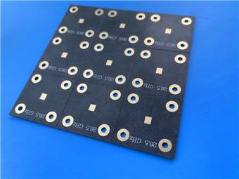
AGC Taconic TLX-6 PTFE Fiberglass Laminate PCB 2-layer 3.5mil ENIG Finish

RF-10 25mil Taconic PCB Materials stands out as a high-performance solution for RF applications. Its exceptional electrical properties, dimensional stability, thermal conductivity, and adhesion characteristics make it an ideal choice for demanding applications.
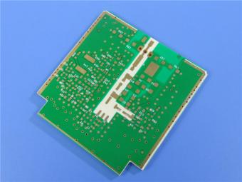
The PCB has a 4-layer hybrid stackup with a 0.5oz+plating ground layer, two 1oz ground layers, and a 0.5oz+plating signal layer.
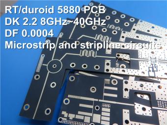
The dimensions of the board are 55.00 x 26.00 mm, with a tolerance of +/- 0.15mm. The board has 16 components, 26 total pads, 9 through-hole pads, 10 top SMT pads, 7 bottom SMT pads, 77 vias, and 82 nets.
Rogers RO4003C PCB is an innovative and advanced circuit board that is made with high-quality materials.
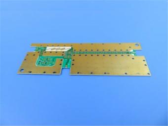
The RO4350B PCB offers a range of benefits that make it an ideal choice for high-frequency applications. Its low dielectric loss and high thermal conductivity make it perfect for high-frequency applications such as RF and microwave circuits.

Bicheng PCB Ships High-Quality PCBs with Shengyi Tg150 ℃ S1000H Material and Advanced Stackup
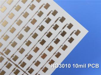
Rogers RO3010 PCB is ideal for a wide range of high-frequency applications, including power amplifiers, filters, couplers, and antennas.
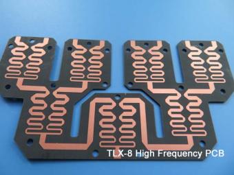
TLX-8 features low dielectric loss, low moisture absorption, and excellent thermal stability, making it ideal for high-frequency and high-speed applications. It has a low dissipation factor, which helps to minimize signal loss and distortion.
 6-11C Shidai Jingyuan, Fuyong, Baoan, Shenzhen, Guangdong, China 518103


For inquiries about our products or pricelist, please leave to us and we will be in touch within 24 hours.
© Copyright: 2026 Shenzhen Bicheng Electronics Technology Co., Ltd.. All Rights Reserved.

IPv6 network supported


