

 Call Us Now !
Tel : +86 755 27374946
Call Us Now !
Tel : +86 755 27374946
 Order Online Now !
Email : info@bichengpcb.com
Order Online Now !
Email : info@bichengpcb.com
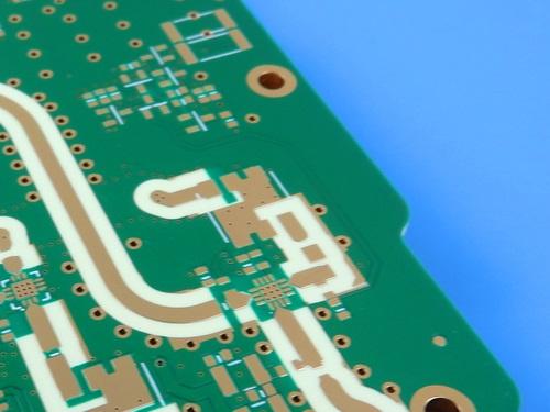
This 8-layer RO4003C + RO4450F PCB is a high-reliability solution for demanding RF and microwave systems.
Item NO.:
BIC-513-v598.0Order(MOQ):
1-10Payment:
T/TProduct Origin:
ChinaShipping Port:
ShenzhenLead Time:
7-10 days
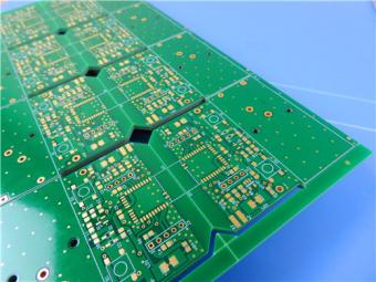
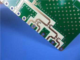
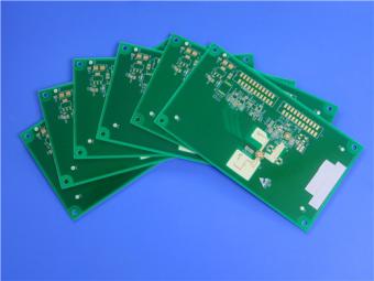
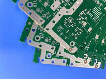
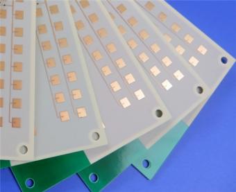
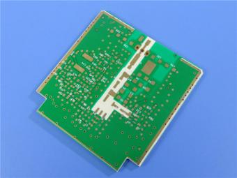
8-layer RO4003C +RO4450F Bondply 5.05mm Thick Immersion Gold Custom High Frequency PCB
Product Overview
This is an 8-layer high-frequency PCB engineered for mission-critical RF, microwave, and millimeter-wave applications. It uses Rogers RO4003C hydrocarbon-ceramic cores and RO4450F bondply for stable dielectric performance, low loss, and excellent multilayer manufacturability.
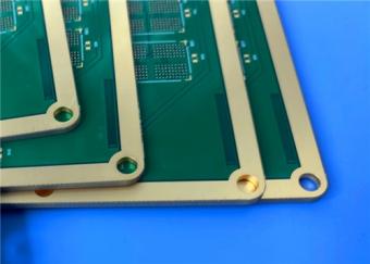
The multilayer board is finished with ENIG for reliable soldering and long-term stability, and fully electrically tested before shipment. It delivers consistent impedance control, minimal signal attenuation, and robust mechanical reliability in commercial and industrial high-frequency systems.
1. PCB Construction Details
This section summarizes the full mechanical, material, and surface-finish configuration of the finished 8-layer board.
|
Item |
Specification |
|
Base Material |
RO4003C + RO4450F |
|
Layer Count |
8 layers |
|
Core Material |
4 × RO4003C cores |
|
Board Dimensions |
91mm × 77mm (1 piece) |
|
Finished Board Thickness |
5.05mm |
|
Finished Copper Weight |
Inner layers: 0.5OZ; Outer layers: 1OZ |
|
Surface Finish |
Immersion Gold (ENIG) |
|
Top Solder Mask |
Green, no silkscreen |
|
Bottom Solder Mask |
Green, white silkscreen |
|
Top Silkscreen |
None |
|
Bottom Silkscreen |
White text |
|
Final QC |
100% electrical test before shipment |
2. PCB Stack-up
This stack-up is designed for impedance consistency, low insertion loss, and reliable multilayer lamination using Rogers4003C cores and RO4450F bondply.

3. RO4003C Datasheet Parameters
These official Rogers specifications define the high-frequency electrical and thermal stability of RO4003C laminate.
|
RO4350B Typical Value |
|||||
|
Property |
RO4350B |
Direction |
Units |
Condition |
Test Method |
|
Dielectric Constant,εProcess |
3.48±0.05 |
Z |
- |
10 GHz/23℃ |
IPC-TM-650 2.5.5.5 Clamped Stripline |
|
Dielectric Constant,εDesign |
3.66 |
Z |
- |
8 to 40 GHz |
Differential Phase Length Method |
|
Dissipation Factortan,δ |
0.0037 |
Z |
- |
10 GHz/23℃ |
IPC-TM-650 2.5.5.5 |
|
Thermal Coefficient of ε |
+50 |
Z |
ppm/℃ |
-50℃to 150℃ |
IPC-TM-650 2.5.5.5 |
|
Volume Resistivity |
1.2 x 10¹⁰ |
- |
MΩ.cm |
COND A |
IPC-TM-650 2.5.17.1 |
|
Surface Resistivity |
5.7 x10⁹ |
- |
MΩ |
COND A |
IPC-TM-650 2.5.17.1 |
|
Electrical Strength |
31.2(780) |
Z |
Kv/mm(v/mil) |
0.51mm(0.020") |
IPC-TM-650 2.5.6.2 |
|
Tensile Modulus |
16,767(2,432) |
X |
MPa(ksi) |
RT |
ASTM D 638 |
|
Tensile Strength |
203(29.5) |
X |
MPa(ksi) |
RT |
ASTM D 638 |
|
Flexural Strength |
255 |
- |
MPa |
- |
IPC-TM-650 2.4.4 |
|
Dimensional Stability |
<0.5 |
X,Y |
mm/m |
after etch+E2/150℃ |
IPC-TM-650 2.4.39A |
|
Coefficient of Thermal Expansion |
10 |
X |
ppm/℃ |
-55℃to288℃ |
IPC-TM-650 2.4.41 |
|
Tg |
>280 |
- |
℃ TMA |
A |
IPC-TM-650 2.4.24.3 |
|
Td |
390 |
- |
℃ TGA |
- |
ASTM D 3850 |
|
Thermal Conductivity |
0.69 |
- |
W/M/oK |
80℃ |
ASTM C518 |
|
Moisture Absorption |
0.06 |
- |
% |
48hrs immersion 0.060" |
ASTM D 570 |
|
Density |
1.86 |
- |
gm/cm3 |
23℃ |
ASTM D 792 |
|
Copper Peel Stength |
0.88 |
- |
N/mm |
after solder float 1 oz. |
IPC-TM-650 2.4.8 |
|
Flammability |
(3)V-0 |
- |
- |
- |
UL 94 |
|
Lead-free Process Compatible |
Yes |
- |
- |
- |
- |
4. RO4003C Typical Applications
RO4003C high frequency PCB is a widely adopted high-frequency laminate that balances electrical performance and processability. It is ideal for:
Its stable Dk, low loss, and copper-matched CTE make it suitable for both single-layer and multilayer RF designs where signal fidelity and thermal stability are required.

5. Conclusion
This 8-layer RO4003C + RO4450F PCB is a high-reliability solution for demanding RF and microwave systems. The combination of Rogers’industry-proven high-frequency materials, tight impedance control, ENIG surface finish, and 100% electrical testing ensures consistent performance in commercial, industrial, and automotive environments.
Compared to standard FR-4 or PTFE-based boards, this design offers lower insertion loss, better thermal stability, and easier manufacturing without special via treatment. It supports high-density routing, reliable lead-free assembly, and long-term operation under fluctuating temperatures and humidity. For engineers seeking a cost-effective, high-performance multilayer RF platform, this board provides a robust, repeatable, and production-ready foundation.
6.RO4003C Multilayer Circuit Processing Guidelines
These guidelines were developed to provide fabricators basic information on processing double-sided and multi-layered printed wiring boards (PWB’s) using RO4003C laminates. Please refer to RO4400 bondply processing guidelines for additional information on inner-layer preparation and multi-layer bonding.
Storage
INNER LAYER PREPARATION
Tooling
Surface Preparation for Photoresist Processing and Copper Etching
Oxide Treatment
Multi-Layer Bonding
DRILLING
Drilling Considerations
Recommended Ranges
|
Surface Speed |
300-500 SFM (90 to 150m/min) |
|
Chip Load |
0.002”-0.004”/rev. (0.05-0.10mm) |
|
Retract Rate |
500 IPM (12.7m/min) for tools less than 0.0135” (0.343mm), 1,000 IPM (25.4 m/min) for all others |
|
Tool Type |
Standard carbide |
|
Tool Life |
2,000-3,000 hits |
CALCULATING SPINDLE SPEED AND INFEED
Example:
QUICK REFERENCE TABLE
|
Tool Diameter |
Spindle Speed (kRPM) |
Infeed Rate (IPM) |
|
0.0100” (0.254mm) |
95.5 |
190 |
|
0.0135” (0.343mm) |
70.7 |
141 |
|
0.0160” (0.406mm) |
95.5 |
190 |
|
0.0197” (0.500mm) |
77.6 |
190 |
|
0.0256” (0.650mm) |
60 |
180 |
|
0.0258” (0.655mm) |
60 |
180 |
|
0.0295” (0.749mm) |
51.8 |
155 |
|
0.0354” (0.899mm) |
43.2 |
130 |
|
0.0394” (1.001mm) |
38.8 |
116 |
|
0.0453” (1.151mm) |
33.7 |
101 |
|
0.0492” (1.257mm) |
31.1 |
93 |
|
0.0531” (1.349mm) |
28.8 |
86 |
|
0.0625” (1.588mm) |
24.5 |
74 |
|
0.0935” (2.350mm) |
16.5 |
50 |
|
0.1250” (3.175mm) |
15 |
45 |
Conditions stated are tapered from 200 SFM and 0.002”chip load up to 400 SFM and 0.003”chip load.
PTH PROCESSING
Surface Preparation
Metal Deposition
COPPER PLATING & OUTER-LAYER PROCESSING
Final Metal Finishes
FINAL CIRCUITIZATION
ROUTING
MAXIMUM STACK HEIGHT
Example:
TOOL TYPE
ROUTING CONDITIONS
QUICK REFERENCE TABLE
Tool DiameterSpindle SpeedLateral Feed Rate
|
Tool Diameter |
Spindle Speed |
Lateral Feed Rate |
|
1/32 |
40k RPM |
50 IPM |
|
1/16 |
25k RPM |
31 IPM |
|
3/32 |
20k RPM |
25 IPM |
|
1/8 |
15k RPM |
25 IPM |
SHELF LIFE


Previous:
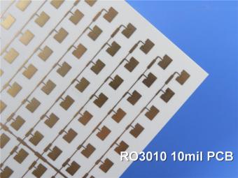
10mil RO3010 2-layer Rogers 3010 PCB ENIG No Solder Mask Black LegendNext:
6-layer RO4003C Laminate + RO4450F PP PCB 1.174mm Finished Thick ENIG Back Drill ViasIf you have questions or suggestions,please leave us a message,we will reply you as soon as we can!
Categories
New Products
12-layer TG200 TU-872 SLK High-Speed FR4 1.68mm PCB with ENIG Impedance Control
12-Layer RO4350B + RO3010 3.14mm Hybrid PCB Nickel-Free EPIG Surface Finish Blind Via
8-Layer Hybrid PCB RO4003C + S1000-2M FR4 with ENIG Surface Finish Blind Via
6-Layer Isola Astra MT77 PCB with Blind Via & Resin Plug Immersion Silver Finish
2-Layer 20mil FSD1020T ENIG High-Frequency PCB with Via Resin Plugged and Capped
4-Layer F4BM265+S1000-2M Material Hyrbid PCB with Blind Via Impedance Control & ENIG
4-Layer Wangling WL-CT338 + FR4 Hybrid PCB ENIG Green Solder Mask White Silkscreen
6-layer Isola 370HR High-Tg FR-4 PCB 2μ" ENIG Impedance Controlled

RF-10 25mil Taconic PCB Materials stands out as a high-performance solution for RF applications. Its exceptional electrical properties, dimensional stability, thermal conductivity, and adhesion characteristics make it an ideal choice for demanding applications.
The PCB has a 4-layer hybrid stackup with a 0.5oz+plating ground layer, two 1oz ground layers, and a 0.5oz+plating signal layer.
The dimensions of the board are 55.00 x 26.00 mm, with a tolerance of +/- 0.15mm. The board has 16 components, 26 total pads, 9 through-hole pads, 10 top SMT pads, 7 bottom SMT pads, 77 vias, and 82 nets.
Rogers RO4003C PCB is an innovative and advanced circuit board that is made with high-quality materials.
The RO4350B PCB offers a range of benefits that make it an ideal choice for high-frequency applications. Its low dielectric loss and high thermal conductivity make it perfect for high-frequency applications such as RF and microwave circuits.
Bicheng PCB Ships High-Quality PCBs with Shengyi Tg150 ℃ S1000H Material and Advanced Stackup
Rogers RO3010 PCB is ideal for a wide range of high-frequency applications, including power amplifiers, filters, couplers, and antennas.
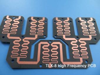
TLX-8 features low dielectric loss, low moisture absorption, and excellent thermal stability, making it ideal for high-frequency and high-speed applications. It has a low dissipation factor, which helps to minimize signal loss and distortion.
 6-11C Shidai Jingyuan, Fuyong, Baoan, Shenzhen, Guangdong, China 518103


For inquiries about our products or pricelist, please leave to us and we will be in touch within 24 hours.
© Copyright: 2026 Shenzhen Bicheng Electronics Technology Co., Ltd.. All Rights Reserved.

IPv6 network supported


