

 Call Us Now !
Tel : +86 755 27374946
Call Us Now !
Tel : +86 755 27374946
 Order Online Now !
Email : info@bichengpcb.com
Order Online Now !
Email : info@bichengpcb.com
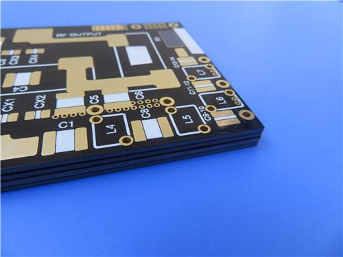
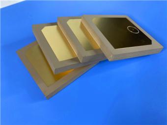
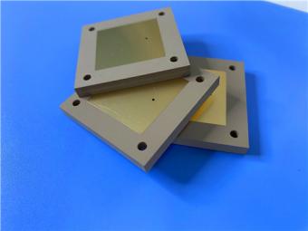
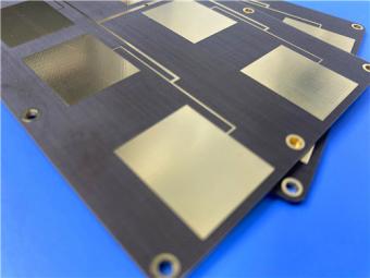
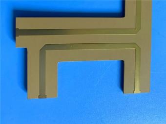
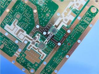
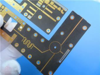
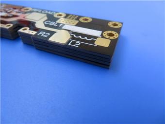
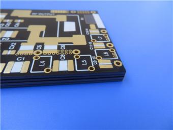
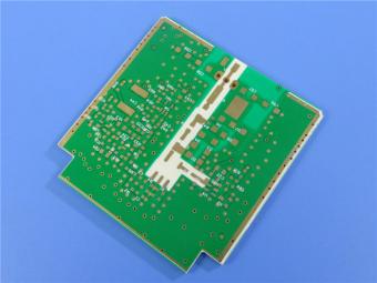
This F4BME275 2-layer pure gold PCB achieves outstanding comprehensive performance through the perfect combination of high-end substrate material and precise manufacturing technology.
Item NO.:
BIC-594-v679.0Order(MOQ):
1-10Payment:
T/TProduct Origin:
ChinaShipping Port:
ShenzhenLead Time:
7-10 days
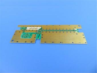
F4BME275 Wangling DK2.75 Laminate 2-Layer 1.6mm Pure Gold RF Custom PCB
Executive Overview
This article presents a comprehensive technical overview of the F4BME275 2-layer RF PCB, a high-frequency printed circuit board built on Wangling's premium PTFE composite laminate with a 1.6 mm finished thickness and5μm pure gold surface finish. Engineered for demanding RF and microwave applications, this 2-layer rigid PCB combines a tightly controlled dielectric constant of 2.75, ultra-low dissipation factor, and reverse-treated foil (RTF) copper to deliver exceptional signal integrity, low passive intermodulation (PIM), and excellent dimensional stability across a wide operating temperature range.
The first section details the PCB construction, layer stackup, and board statistics for this specific 103×76 mm reference design. The second section provides an in-depth, standalone datasheet analysis of theF4BME275 copper-clad laminate(CCL) material itself, covering electrical, mechanical, thermal, and environmental specifications. Both sections conclude independently to support engineers and procurement teams in evaluating the board and the base material separately.
Part 1: F4BME275 2-Layer PCB—Product Specification
1.1 PCB Construction Details
The table below summarizes the core manufacturing specifications of this 2-layer RF PCB, including board dimensions, trace geometry, copper weight, surface finish, and quality control criteria that define its as-built configuration.
|
Parameter |
Specification |
|
Layer Count |
2-layer RF PCB |
|
Board Dimensions |
103 mm × 76 mm per panel, ±0.15mm tolerance |
|
Minimum Trace/Space |
6/9 mils (0.152/0.229 mm) |
|
Minimum Hole Size |
0.5 mm |
|
Finished Board Thickness |
1.6 mm (±10%) |
|
Finished Copper Weight |
1 oz (1.4 mils / 35 μm) on outer layers |
|
Via Plating Thickness |
20 μm (minimum) |
|
Surface Finish |
Pure Gold (5 μm / 197 μinches) |
|
Top Silkscreen |
White |
|
Bottom Silkscreen |
None |
|
Top Solder Mask |
Black |
|
Bottom Solder Mask |
None |
|
Electrical Testing |
100% electrical test performed prior to shipment |
|
Artwork Type |
Gerber RS-274-X |
|
Quality Standard |
IPC-Class-2 |
|
Availability |
Worldwide |
1.2 PCB Layer Stackup
This 2-layer rigid PCB employs a symmetric stackup built around a single F4BME275 core with 35μm copper cladding on both sides, yielding a total finished board thickness of 1.6 mm.
|
Layer Position |
Material |
Thickness |
Unit |
|
Top Copper (Layer 1) |
Copper (RTF) |
35 |
μm |
|
Core |
F4BME275 |
1.524 |
mm (60 mils) |
|
Bottom Copper (Layer 2) |
Copper (RTF) |
35 |
μm |
1.3 PCB Design Statistics
The reference design populated on this board contains 37 components distributed across 7 signal nets, with a mix of through-hole and surface-mount pads optimized for RF signal routing and mechanical mounting.
|
Metric |
Count |
|
Components |
37 |
|
Total Pads |
56 |
|
Thru-Hole Pads |
37 |
|
Top SMT Pads |
19 |
|
Bottom SMT Pads |
0 |
|
Vias |
21 |
|
Nets |
7 |
1.4 Material & Performance Highlights
At the heart of this PCB lies the F4BME275 laminate, a PTFE (polytetrafluoroethylene) composite reinforced with woven fiberglass cloth and clad with reverse-treated foil (RTF) copper. Compared with standard ED-copper laminates such as the F4BM275 variant, the RTF copper surface delivers three measurable advantages critical to high-frequency designs: lower passive intermodulation (PIM≤ −159 dBc), finer and more consistent etch definition for 6-mil trace geometries, and reduced conductor loss at microwave frequencies.
The dielectric constant is tightly held at 2.75 with a tolerance of only±0.05 at 10 GHz, providing designers with predictable impedance behavior. With a dissipation factor of just 0.0015 at 10 GHz (0.0021 at 20 GHz), insertion loss remains exceptionally low even on longer transmission-line runs. The temperature coefficient of dielectric constant (TCDk) is−92 ppm/°C across−55°C to +150°C, ensuring that filter and antenna responses drift minimally over environmental extremes.
Mechanically, the 1.524 mm core contributes to a rigid, flat board with an in-plane CTE of only 14–16 ppm/°C, closely matched to copper and reducing thermal stress on solder joints and plated through holes. The 20μm via plating and IPC-Class-2 workmanship standard further support long-term reliability in field-deployed equipment.
1.5 Surface Finish & Assembly Compatibility
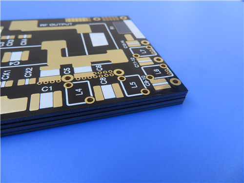
The 5μm pure gold finish provides excellent solderability, low contact resistance, and corrosion resistance—especially valuable for edge-launch connectors, RF probes, and gold-plated coaxial interfaces common in microwave test fixtures and base-station feed networks. Unlike immersion gold (ENIG), the thicker pure gold layer here withstands repeated mating cycles and is well-suited to boards that serve as test platforms or high-reliability sub-assemblies. The single-sided solder mask (black, top side only) leaves the bottom copper fully exposed for applications requiring direct ground contact, thermal bonding to a chassis, or microstrip characterization setups.
1.6 Typical Applications
This F4BME275 2-layer PCB configuration is targeted at RF and microwave subsystems where controlled impedance, low loss, and PIM performance are primary requirements. Representative use cases include:
1.7 PCB Section—Conclusion
This F4BME275 2-layer pure gold PCB achieves outstanding comprehensive performance through the perfect combination of high-end substrate material and precise manufacturing technology. Different from ordinary gold-plated PCBs, the 5μm thick pure gold finish completely avoids signal attenuation and PIM deterioration caused by nickel barrier layers in traditional ENIG processes, ensuring ultra-low passive intermodulation and stable high-frequency conductivity. The symmetrical stackup structure guarantees excellent flatness and dimensional stability, while fine-line processing capability and standardized electrical testing eliminate circuit defects. Tailored for high-frequency RF scenarios, this F4BME275 high frequency PCB delivers reliable signal integrity, low loss and high assembly compatibility, fully meeting the stringent performance requirements of microwave communication and radar equipment.
Part 2: In-Depth Introduction of F4BME275 CCL Substrate Material
2.1 Material Overview
The F4BME275 copper-clad laminate is a high-performance PTFE (Polytetrafluoroethylene) composite material engineered by Wangling specifically for demanding RF and microwave applications. The laminate is constructed from woven fiberglass cloth, PTFE resin, and PTFE films, precision-formulated and processed under stringent manufacturing controls to ensure consistent and superior electrical properties.
2.2 Product Family Introduction
The Wangling F4BME275 is part of Wangling's advanced F4B series of PTFE composites. The material platform has been refined over multiple generations, with F4BME275 specifically designed to address the limitations of earlier materials (such as F4B220) while providing a reliable, high-performance domestic alternative to comparable imported laminates from Rogers Corporation, Taconic, and Arlon.
Key Family Distinctions:
|
Product |
Copper Foil Type |
PIM Performance |
Primary Application |
|
F4BM |
ED (Electrodeposited) |
Not specified / standard |
General RF applications |
|
F4BME |
RTF (Reverse-Treated Foil) |
Superior |
Low-PIM, high-frequency applications |
|
F4BME275 |
RTF (Reverse-Treated Foil) |
≤ -159 dBc |
Premium low-PIM, precision RF circuits |
2.3 Complete F4BME275 Datasheet Parameter Table
The following table presents the complete technical data for F4BME275 as published by Wangling:
|
Property / Characteristic |
Test Condition |
Unit |
F4BME275 Value |
|
Dielectric Constant (Typical) |
10 GHz, 23°C, 50% RH |
– |
2.75 |
|
Dielectric Constant Tolerance |
– |
– |
± 0.05 |
|
Dissipation Factor (Loss Tangent, Typical) |
10 GHz |
– |
0.0015 |
|
20 GHz |
– |
0.0021 |
|
|
Temperature Coefficient of Dk (TCDk) |
-55°C to +150°C |
ppm/°C |
-92 |
|
Peel Strength (1 oz RTF) |
F4BME, after solder float |
N/mm |
≥ 1.6 |
|
Volume Resistivity |
Normal state (23°C, 50% RH) |
MΩ·cm |
≥ 6 × 10⁶ |
|
Surface Resistance |
Normal state |
MΩ |
≥ 1 × 10⁶ |
|
Electrical Strength (Z-direction) |
5 kV, 500 V/s ramp, 50 Hz AC |
MV/m |
> 28 |
|
Breakdown Voltage (XY-direction) |
5 kV, 500 V/s ramp |
kV |
> 35 |
|
CTE – XY Direction |
-55°C to 288°C |
ppm/°C |
14 ~ 16 |
|
CTE – Z Direction |
-55°C to 288°C |
ppm/°C |
112 |
|
Thermal Stress |
260°C, 10 sec, 3 exposures |
– |
No delamination |
|
Water Absorption |
20±2°C, 24 hours |
% |
≤ 0.08 |
|
Density |
Room temperature |
g/cm³ |
2.28 |
|
Continuous Operating Temperature |
In air, no load |
°C |
-55 to +260 |
|
Thermal Conductivity (Z-direction) |
– |
W/(M·K) |
0.38 |
|
PIM Performance |
Two-tone, 43 dBm |
dBc |
≤ -159 |
|
Flammability |
UL 94 standard |
Rating |
V-0 |
|
Material Composition |
– |
– |
PTFE + Woven Fiberglass + RTF Copper Foil |
2.4 Available Copper Foil Options and Material Thicknesses
|
Copper Type |
Availability |
Thickness Options |
|
ED Copper (F4BM) |
Standard |
0.5 oz (0.018mm), 1 oz (0.035mm), 1.5 oz (0.05mm), 2 oz (0.07mm) |
|
RTF Copper (F4BME) |
Premium (this PCB) |
0.5 oz (0.018mm), 1 oz (0.035mm) – 1 oz used in this PCB |
2.5 Standard Panel Sizes Available:
|
Dimensions |
Type |
|
460×610 mm |
Standard |
|
500×600 mm |
Standard |
|
850×1200 mm |
Standard |
|
914×1220 mm |
Standard |
|
1000×1200 mm |
Standard |
|
300×250 mm |
Custom (non-standard) |
|
350×380 mm |
Custom (non-standard) |
|
500×500 mm |
Custom (non-standard) |
|
840×840 mm |
Custom (non-standard) |
|
1000×1500 mm |
Custom (non-standard) |
Note: For total thicknesses≥4.0mm or≤0.2mm, maximum panel size is limited to 500×610mm.
2.6 Dielectric Thickness Options (1 oz RTF Copper)
The following table provides the standard thickness options available for the F4BME series. This PCB uses the 1.524mm (60 mil) dielectric thickness option.
|
Thickness (mm) |
Description |
Tolerance (mm) |
|
0.1 |
Dielectric only |
±0.01 |
|
0.127 |
Dielectric only |
±0.01 |
|
0.2 |
Nominal |
±0.02 |
|
0.25 |
Nominal |
±0.02 |
|
0.5 |
Nominal |
±0.04 |
|
0.508 |
Nominal |
±0.04 |
|
0.762 |
Nominal |
±0.05 |
|
0.8 |
Nominal |
±0.05 |
|
1 |
Nominal |
±0.05 |
|
1.5 |
Nominal |
±0.06 |
|
1.524 |
Nominal (this PCB) |
±0.06 |
|
1.575 |
Nominal |
±0.06 |
|
2 |
Nominal |
±0.08 |
|
2.5 |
Nominal |
±0.08 |
|
3 |
Nominal |
±0.09 |
|
4 |
Nominal |
±0.10 |
|
5 |
Nominal |
±0.10 |
|
6 |
Nominal |
±0.12 |
|
8 |
Nominal |
±0.15 |
|
10 |
Nominal |
±0.18 |
|
12 |
Nominal |
±0.20 |
Important Note: For dielectric constants≤2.65, the minimum available dielectric thickness is 0.1mm. For dielectric constants between 2.7 and 3.0, the minimum available dielectric thickness is 0.2mm. This relationship exists because higher fiberglass content required for higherεr values reduces the minimum practical thickness due to fiberglass weave constraints.
2.7 Metal-Backed Variants–F4BME275-AL / CU
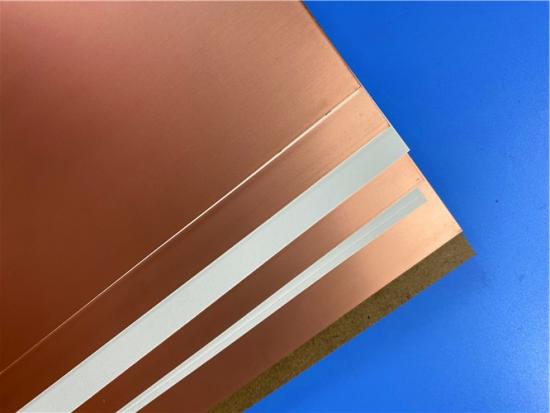
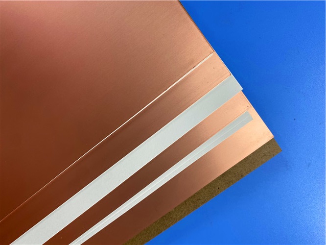
For applications requiring heat dissipation, shielding, or mechanical reinforcement, F4BME275 is available with an integrated aluminum or copper base layer. These are designated:
Metal-backed versions provide efficient heat spreading for high-power amplifiers and reduce ground-plane impedance while maintaining the low-loss PTFE dielectric interface.
2.8 Typical Applications (CCL Level)
2.9 CCL Conclusion
Wangling F4BME275 is a premium PTFE-based copper-clad laminate that delivers a compelling balance of electrical performance, thermal stability, and manufacturing versatility. Its controlled Dk = 2.75±0.05, low Df = 0.0015 at 10 GHz, and RTF copper foil with PIM≤-159 dBc make it a superior choice for high-frequency, high-reliability applications. Unlike standard ED copper laminates, the RTF foil ensures finer etching resolution and lower conductor loss, directly translating to better signal integrity and improved passive intermodulation performance. Combined with flexible thickness options from 0.1 mm to 12.0 mm, multiple panel sizes, and aluminum/copper-backed variants, F4BME275 offers designers a robust platform for innovative RF and microwave system designs.
As a domestic, high-performance alternative to imported laminates such as Rogers RO4000® series or Taconic TLY® series, F4BME275 enables cost-effective, scalable production without compromising on electrical or mechanical quality. Its long-term reliability, proven by stringent thermal stress, moisture resistance, and electrical testing, positions it as a trusted material for the next generation of wireless infrastructure, aerospace, and defense electronics.

Previous:
Wangling 5mil 0.127mm TFA300 Core 2-layer Immersion Gold Green Solder Mask PCBNext:
Wangling F4BTD350S High Frequency PCB 2-layer 20mil Thick ENIG DK3.5 SubstrateIf you have questions or suggestions,please leave us a message,we will reply you as soon as we can!
Categories
New Products
Wangling TP2200 PCB 0.8mm Substrate Immersion Gold 2-Layer High-Dk (Dk 22) RF Board
Rogers TMM10 PCB 5.08mm Core ENIG 2-Layer High-Dk Microwave Board
Taconic TLX-8 PCB 50mil ENIG 2-Layer High-Frequency RF Circuit Board
Wangling TF440 25mil DK4.4 Laminate Immersion Gold 2-Layer Copper-filling Vias PCB
RO4360G2 Rogers 12mil ENEPIG 2-Layer DK6.15 High Frequency Custom PCB
Wangling F4BTMS220 2-Layer DK2.2 PCB 10 mil Core with Immersion Gold
Wangling F4BTME350 10mil DK3.5 High Frequency Substrate PCB 2-Layer Immersion Gold
Wangling F4BTM300 Custom 2-layer PCB 20mil DK3.0 Substrate with Immersion Gold

RF-10 25mil Taconic PCB Materials stands out as a high-performance solution for RF applications. Its exceptional electrical properties, dimensional stability, thermal conductivity, and adhesion characteristics make it an ideal choice for demanding applications.
The PCB has a 4-layer hybrid stackup with a 0.5oz+plating ground layer, two 1oz ground layers, and a 0.5oz+plating signal layer.
The dimensions of the board are 55.00 x 26.00 mm, with a tolerance of +/- 0.15mm. The board has 16 components, 26 total pads, 9 through-hole pads, 10 top SMT pads, 7 bottom SMT pads, 77 vias, and 82 nets.
Rogers RO4003C PCB is an innovative and advanced circuit board that is made with high-quality materials.
The RO4350B PCB offers a range of benefits that make it an ideal choice for high-frequency applications. Its low dielectric loss and high thermal conductivity make it perfect for high-frequency applications such as RF and microwave circuits.

Bicheng PCB Ships High-Quality PCBs with Shengyi Tg150 ℃ S1000H Material and Advanced Stackup
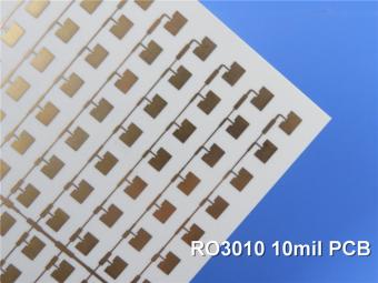
Rogers RO3010 PCB is ideal for a wide range of high-frequency applications, including power amplifiers, filters, couplers, and antennas.
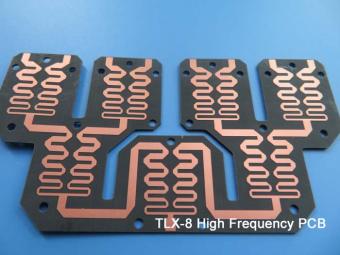
TLX-8 features low dielectric loss, low moisture absorption, and excellent thermal stability, making it ideal for high-frequency and high-speed applications. It has a low dissipation factor, which helps to minimize signal loss and distortion.
 6-11C Shidai Jingyuan, Fuyong, Baoan, Shenzhen, Guangdong, China 518103


For inquiries about our products or pricelist, please leave to us and we will be in touch within 24 hours.
© Copyright: 2026 Shenzhen Bicheng Electronics Technology Co., Ltd.. All Rights Reserved.

IPv6 network supported


