

 Call Us Now !
Tel : +86 755 27374946
Call Us Now !
Tel : +86 755 27374946
 Order Online Now !
Email : info@bichengpcb.com
Order Online Now !
Email : info@bichengpcb.com
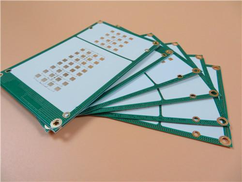
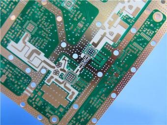
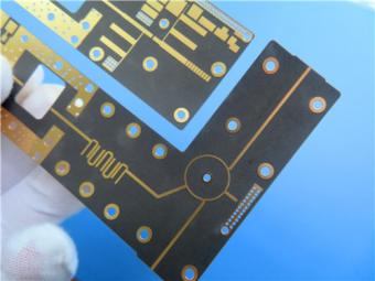
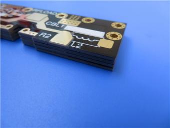
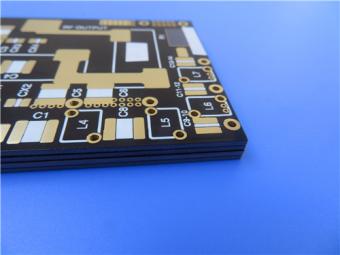
The 5mil TFA3002-layer PCB combines an ultra-thin form factor with aerospace-grade dielectric performance, making it a compelling solution for high-frequency designs that demand both compactness and reliability.
Item NO.:
BIC-598-v683.0Order(MOQ):
1-10Payment:
T/TProduct Origin:
ChinaShipping Port:
ShenzhenLead Time:
7-10 days
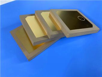
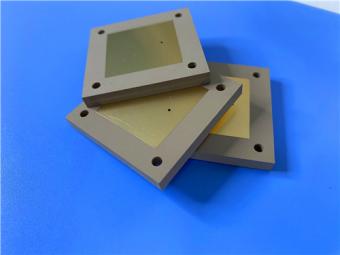
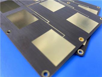
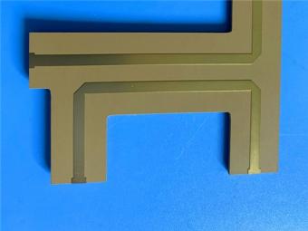
Wangling 5mil 0.127mm TFA300 Core 2-layer ImmersionGold Green Solder Mask PCB
Executive Overview
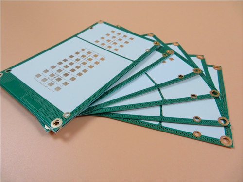
This is our 5mil TFA300 2-layer printed circuit board with immersion gold surface finish. Built on Wangling TFA300 PTFE-ceramic composite substrate, this ultra-thin 0.2 mm rigid PCB is engineered specifically for high-frequency applications requiring tight dielectric control, low insertion loss, and exceptional thermal-mechanical stability. The board measures 87x 54 mm per unit, features 1 oz copper on both outer layers, and is manufactured to IPC Class 2 quality standards with 100% electrical testing prior to shipment.
Below, the PCB product specifications are detailed in full, followed by an independent deep-dive section on the TFA300 copper-clad laminate (CCL) material, including its complete datasheet, material science background, and available configuration options.
1. PCB Product Description
1.1 Product Introduction
The 5mil TFA300 2-layer ENIG PCB is a high-frequency rigid circuit board designed for microwave, radar, and aerospace-grade applications where signal integrity and phase stability are mission-critical. Unlike conventional FR-4 boards, this product employs a PTFE-ceramic dielectric core (TFA300, Dk 3.00) that delivers consistent electrical performance from L-band through millimeter-wave frequencies up to 77 GHz. With a finished board thickness of only 0.2 mm and a core dielectric of 0.127 mm (5 mil), the board achieves a compact, low-profile form factor while maintaining full 1 oz copper weight on both layers for sufficient current-carrying capacity and controlled-impedance line geometries. The immersion gold (ENIG) surface finish provides excellent solderability, corrosion resistance, and a flat contact surface ideal for high-frequency connectors and fine-pitch SMT assembly.
1.2 PCB Construction Details
The table below summarizes the complete construction parameters of this PCB, covering base material, layer configuration, dimensional tolerances, conductor geometry, plating specifications, and surface finish.
|
Parameter |
Specification |
|
Base Material |
TFA300 (PTFE Ceramic Composite) |
|
Layer Count |
2 layers |
|
Board Dimensions |
87 mm × 54 mm per piece, ±0.15 mm tolerance |
|
Minimum Trace / Space |
6 mil / 8 mil |
|
Minimum Hole Size |
0.4 mm |
|
Blind Vias |
None |
|
Finished Board Thickness |
0.2 mm |
|
Finished Copper Weight |
1 oz (1.4 mil / 35 μm) outer layers |
|
Via Plating Thickness |
20 μm |
|
Surface Finish |
Immersion Gold (ENIG) |
|
Top Silkscreen |
No |
|
Bottom Silkscreen |
No |
|
Top Solder Mask |
Green |
|
Bottom Solder Mask |
No |
|
Electrical Testing |
100% tested prior to shipment |
|
Quality Standard |
IPC-Class-2 |
|
Artwork Format |
Gerber RS-274-X |
|
Availability |
Worldwide |
1.3 PCB Stackup
This 2-layer rigid PCB uses a symmetric stackup with identical 35μm copper cladding on both sides of a 0.127 mm TFA300 core, ensuring balanced thermal expansion and straightforward impedance modeling.
|
Layer |
Material |
Thickness |
|
Copper Layer 1 (Top) |
RTF Copper Foil |
35 μm (1 oz) |
|
Core |
TFA300 Dielectric |
0.127 mm (5 mil) |
|
Copper Layer 2 (Bottom) |
RTF Copper Foil |
35 μm (1 oz) |
1.4 PCB Statistics
The following table quantifies the board's component and net density, reflecting a focused, low-component-count design typical of RF signal-path or power-amplifier circuitry.
|
Category |
Count |
|
Total Components |
18 |
|
Total Pads |
36 |
|
Through-Hole Pads |
19 |
|
Top SMT Pads |
17 |
|
Bottom SMT Pads |
0 |
|
Vias |
6 |
|
Electrical Nets |
2 |
1.5 Key Performance Differentiators
1) Tight Dielectric Control for Predictable Impedance:
TFA300 holds a Dk tolerance of±0.04 at 10 GHz, among the tightest in the industry for a Dk-3.0 material. For a 50Ωmicrostrip line on 5 mil dielectric, this translates to an impedance variation of less than±1Ω, enabling designers to rely on simulation results without over-engineering for material uncertainty.
2) Ultra-Low Loss Across Broad Frequencies:
With a dissipation factor of 0.001 at 10 GHz and 20 GHz, and only 0.0012 at 40 GHz, the material preserves signal power at frequencies where FR-4 (typically Df≈0.02 at 10 GHz) would dissipate energy as heat. For a 50 mm signal path at 20 GHz, the insertion loss advantage over FR-4 is substantial and directly improves link budget.
3) Copper-Matched CTE for Via Reliability:
The in-plane coefficient of thermal expansion is 18 ppm/°C—nearly identical to that of copper foil (~17 ppm/°C). This matching dramatically reduces shear stress on plated through-holes during thermal cycling, which is why the board achieves IPC Class 2 reliability even with a 20μm via plating specification. The Z-axis CTE of 30 ppm/°C is also exceptionally low for a PTFE-based material, further safeguarding via integrity.
4) Excellent Thermal and Environmental Stability
With a TCDK of only−8 ppm/°C over the−55°C to +150°C range, the dielectric constant shifts by less than 0.17% across the full operating temperature window. For phase-sensitive arrays and frequency-selective circuits, this stability directly translates to predictable phase response—a critical requirement for phased-array antennas and airborne radar systems.
5) Immersion Gold for High-Frequency Contacts
The ENIG surface finish provides a nickel barrier layer beneath a thin gold coating, ensuring low contact resistance, consistent solder joint quality, and long shelf life. For edge-launch connectors and RF probes commonly used in high-frequency testing, the flat, uniform gold surface is preferable to HASL or OSP finishes.
1.6 Typical Applications
This TFA300 high frequency PCB configuration is well-suited for the following application domains:
1)Aerospace & Avionics: In-cabin equipment, aircraft radar subsystems, satellite payload components where low outgassing and radiation tolerance are required.
2)Microwave & Antenna Systems: Phase-sensitive antennas, microstrip patch arrays, and beamforming networks demanding stable Dk across temperature.
3)Radar Systems: Early-warning radar, airborne radar, and automotive radar modules operating up to 77 GHz.
4)Satellite Communications & Navigation: LNB circuits, filters, and power amplifiers in ground-segment and space-borne equipment.
5)RF Power Amplifiers: Compact PA stages where low-loss dielectric and thermal stability directly impact efficiency and linearity.
1.7 PCB Conclusion
The 5mil TFA3002-layer PCB combines an ultra-thin form factor with aerospace-grade dielectric performance, making it a compelling solution for high-frequency designs that demand both compactness and reliability. Its 1 oz copper weight, 6/8 mil trace/space capability, and 0.4 mm minimum drill size provide sufficient routing headroom for typical RF sub-circuits, while theTFA300 substrate delivers Dk stability, low loss, and copper-matched CTE that FR-4 and even many mid-range high-frequency materials cannot match. Manufactured to IPC Class 2 standards with 100% electrical testing, thisWanglingboard offers a validated, production-ready platform for microwave, radar, and aerospace applications where every dB and every degree of phase shift matters.
2. CCL Material Deep Dive—TFA300 PTFE-Ceramic Composite Substrate
2.1 Material Introduction
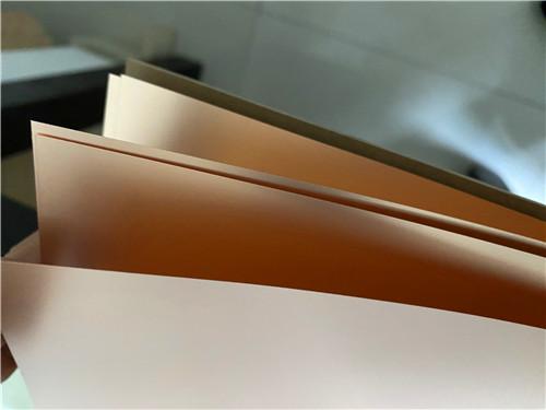
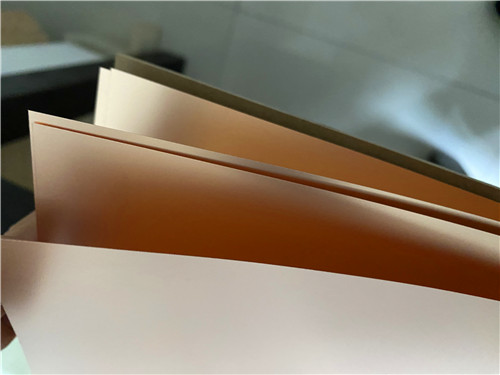
TFA300 is a member of theWangling TFA seriesof polytetrafluoroethylene (PTFE) ceramic composite dielectric substrates, manufactured by Taizhou Wangling Insulating Materials Factory. Unlike traditional glass-fiber-reinforced laminates that impregnate woven fiberglass cloth with resin, the TFA series uses a proprietary manufacturing process in which nano-ceramic fillers are uniformly dispersed within PTFE resin to form prepreg sheets, which are then laminated under specialized pressing conditions. The result is a glass-fiber-free substrate with exceptional electrical uniformity, minimal anisotropy across X, Y, and Z axes, and dielectric properties that remain remarkably stable across frequency and temperature.
The TFA substrate series offers four dielectric constant grades—TFA294 (Dk 2.94), TFA300 (Dk 3.00), TFA615 (Dk 6.15), and TFA1020 (Dk 10.2)—allowing designers to select the exact Dk value for their impedance and antenna-size requirements. TFA300, at Dk 3.00, is the most versatile grade for general microwave and millimeter-wave circuits, balancing line width practicality with low-loss performance.
2.2 Technology & Composition Advantages
1) No Glass-Weave Effect:
Because TFA300 contains no fiberglass cloth, electromagnetic waves propagating through the dielectric do not encounter the periodic variations in Dk caused by woven glass bundles. This eliminates the "glass-weave effect"—a known source of impedance skew and phase jitter in high-speed digital and mmWave circuits built on conventional FR-4 or glass-reinforced hydrocarbon laminates. For differential pairs and phased-array elements, the absence of weave-induced skew is a significant performance advantage.
2) Uniform Nano-Ceramic Filler:
The material uses a high loading of specially formulated nano-ceramic particles uniformly distributed throughout the PTFE matrix. This homogeneous filler distribution is what enables the tight±0.04 Dk tolerance and the low TCDK of−8 ppm/°C. Batch-to-batch consistency is a hallmark of the TFA series, reducing design margins and improving yield for production runs.
3) Low Outgassing & Radiation Resistance:
TFA300 meets aerospace vacuum outgassing requirements (low TML / CVCM) and maintains stable dielectric and physical properties after radiation exposure. These characteristics qualify the material for space-borne and high-altitude avionics applications where conventional organic substrates risk degradation.
4) Standard PTFE Process Compatibility:
Despite its advanced composition, TFA300 can be processed using standard PTFE PCB fabrication techniques. Its good mechanical and physical properties support multilayer and high-layer-count stackups, backplane construction, dense via drilling, and fine-line patterning—providing design flexibility beyond simple two-layer boards.
2.3 TFA300 Complete Datasheet
The table below provides the full electrical, thermal, mechanical, and environmental specifications for the TFA300 CCL material, as published by the manufacturer. All values are typical measurements tested per IPC-TM-650 or GB/T 4722-2017 methods unless otherwise noted.
|
Property |
Test Condition |
Unit |
TFA300 Value |
|
Dielectric Constant (Typical) |
10 GHz, Z-direction |
— |
3 |
|
Dielectric Constant (Design Value) |
10 GHz, microstrip |
— |
3 |
|
Dielectric Constant Tolerance |
— |
— |
±0.04 |
|
Dissipation Factor (Df) |
10 GHz |
— |
0.001 |
|
Dissipation Factor (Df) |
20 GHz |
— |
0.001 |
|
Dissipation Factor (Df) |
40 GHz |
— |
0.0012 |
|
Temperature Coefficient of Dk (TCDK) |
-55°C ~ 150°C |
ppm/°C |
-8 |
|
Peel Strength |
1 oz RTF copper foil |
N/mm |
> 1.6 |
|
Volume Resistivity |
Normal condition |
MΩ·cm |
≥ 5×10⁷ |
|
Surface Resistivity |
Normal condition |
MΩ |
≥ 5×10⁷ |
|
Electric Strength (Z-direction) |
5 kW, 500 V/s |
kV/mm |
> 32 |
|
Breakdown Voltage (XY-direction) |
5 kW, 500 V/s |
kV |
> 40 |
|
CTE (X / Y direction) |
-55°C ~ 288°C |
ppm/°C |
18 / 18 |
|
CTE (Z direction) |
-55°C ~ 288°C |
ppm/°C |
30 |
|
Thermal Stress |
260°C, 10 s, 3 cycles |
— |
No delamination |
|
Moisture Absorption |
20±2°C, 24 hours |
% |
0.04 |
|
Density |
Room temperature |
g/cm³ |
2.15 |
|
Continuous Operating Temperature |
Thermal chamber |
°C |
-55 ~ +260 |
|
Thermal Conductivity |
Z-direction |
W/(m·K) |
0.6 |
|
Flammability |
— |
UL-94 |
V-0 |
|
Decomposition Temperature (Td) |
Onset |
°C |
498 |
|
Material Composition |
— |
— |
PTFE + Ceramic |
2.4 Available Copper Foil Options
TFA300 is offered with several copper foil configurations to suit different design requirements:
1) Standard Copper Thickness:
0.5 oz (18μm) and 1 oz (35μm) are standard; other thicknesses are available by custom order.
2) Standard Foil Type:
RTF (Reverse Treat Foil) low-roughness copper is supplied as standard. RTF reduces conductor loss at high frequencies compared to standard rolled-annealed or high-profile ED foils, while maintaining excellent peel strength (>1.6 N/mm for 1 oz).
3) Rolled Annealed (RA) Copper Foil:
Available as an option for applications requiring the smoothest possible conductor surface for minimum skin-effect loss at mmWave frequencies.
4) Embedded 50ΩResistor Foil:
TFA294 and TFA300 can be supplied with an embedded resistive copper foil. The resistor film is a nickel-phosphorus (Ni-P) alloy, 0.2μm thick, with a sheet resistance of 50±5Ωper square. This enables integrated termination resistors directly in the substrate, eliminating discrete components and improving high-frequency performance.
5) Metal Base Options:
TFA series laminates can be paired with copper or aluminum bases for enhanced thermal management in high-power amplifier designs.
2.5 Standard Panel Sizes & Dielectric Thicknesses
Standard Panel Sizes:
305×460 mm (12"×18") and 460×610 mm (18"×24"). Custom sizes are available upon request.
Dielectric Thickness&Tolerance Range:
The TFA series starts at 0.127 mm (5 mil) as the thinnest standard option and is available in multiples of 0.127 mm. The 5 mil (0.127 mm) core used in the featured PCB represents the thinnest standard gauge, ideal for compact 50Ωmicrostrip geometries and thin-form-factor assemblies.
|
Thickness mm(mil) |
Tolerance mm(mil) |
Thickness mm(mil) |
Tolerance mm(mil) |
|
0.127mm(5.0mil) |
±0.0127mm(0.5mil) |
1.905mm(75mil) |
±0.09mm(3.5mil) |
|
0.254mm(10mil) |
±0.02mm(1.0mil) |
2.03mm(80mil) |
±0.09mm(3.5mil) |
|
0.508mm(20mil) |
±0.03mm(1.19mil) |
2.54mm(100mil) |
±0.13mm(5.0mil) |
|
0.635mm(25mil) |
±0.03mm(1.58mil) |
3.175mm(125mil) |
±0.20mm(8.0mil) |
|
0.762mm(30mil) |
±0.04mm(1.58mil) |
3.81mm(150mil) |
±0.25mm(10.0mil) |
|
1.016mm(40mil) |
±0.05mm(2.0mil) |
4.06mm(160mil) |
±0.25mm(10.0mil) |
|
1.270mm(50mil) |
±0.05mm(2.0mil) |
5.08mm(200mil) |
±0.25mm(10.0mil) |
|
1.524mm(60mil) |
±0.07mm(2.5mil) |
6.35mm(250mil) |
±0.32mm(12.6mil) |
2.6 CCL Conclusion
TFA300 stands out as a high-performance PTFE-ceramic composite substrate that delivers aerospace-grade electrical and thermal-mechanical performance at a Dk of 3.00—the sweet spot for many microwave and mmWave designs. Its glass-fiber-free composition eliminates weave-induced skew, its±0.04 Dk tolerance enables tight impedance control, and its copper-matched CTE of 18 ppm/°C ensures long-term via reliability under thermal cycling. With support for RTF low-loss foil, embedded resistor foil, and metal-base configurations, the material adapts to a wide range of high-frequency design requirements. For engineers seeking a domestic alternative to imported high-frequency laminates without compromising on Dk stability, loss performance, or reliability, TFA300 is a technically competitive and commercially viable choice.

Previous:
F4BTM298 PCB 10mil Wangling Laminate 2-Layer Immersion Gold Black Solder MaskNext:
F4BME275 Wangling DK2.75 Laminate 2-Layer 1.6mm Pure Gold RF Custom PCBIf you have questions or suggestions,please leave us a message,we will reply you as soon as we can!
Categories
New Products
Wangling TP2200 PCB 0.8mm Substrate Immersion Gold 2-Layer High-Dk (Dk 22) RF Board
Rogers TMM10 PCB 5.08mm Core ENIG 2-Layer High-Dk Microwave Board
Taconic TLX-8 PCB 50mil ENIG 2-Layer High-Frequency RF Circuit Board
Wangling TF440 25mil DK4.4 Laminate Immersion Gold 2-Layer Copper-filling Vias PCB
RO4360G2 Rogers 12mil ENEPIG 2-Layer DK6.15 High Frequency Custom PCB
Wangling F4BTMS220 2-Layer DK2.2 PCB 10 mil Core with Immersion Gold
Wangling F4BTME350 10mil DK3.5 High Frequency Substrate PCB 2-Layer Immersion Gold
Wangling F4BTM300 Custom 2-layer PCB 20mil DK3.0 Substrate with Immersion Gold

RF-10 25mil Taconic PCB Materials stands out as a high-performance solution for RF applications. Its exceptional electrical properties, dimensional stability, thermal conductivity, and adhesion characteristics make it an ideal choice for demanding applications.
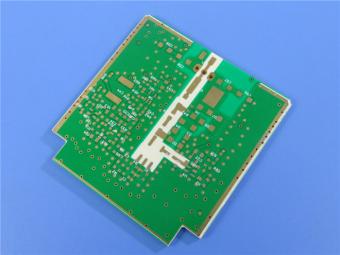
The PCB has a 4-layer hybrid stackup with a 0.5oz+plating ground layer, two 1oz ground layers, and a 0.5oz+plating signal layer.
The dimensions of the board are 55.00 x 26.00 mm, with a tolerance of +/- 0.15mm. The board has 16 components, 26 total pads, 9 through-hole pads, 10 top SMT pads, 7 bottom SMT pads, 77 vias, and 82 nets.
Rogers RO4003C PCB is an innovative and advanced circuit board that is made with high-quality materials.
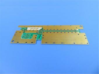
The RO4350B PCB offers a range of benefits that make it an ideal choice for high-frequency applications. Its low dielectric loss and high thermal conductivity make it perfect for high-frequency applications such as RF and microwave circuits.

Bicheng PCB Ships High-Quality PCBs with Shengyi Tg150 ℃ S1000H Material and Advanced Stackup
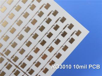
Rogers RO3010 PCB is ideal for a wide range of high-frequency applications, including power amplifiers, filters, couplers, and antennas.
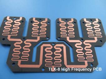
TLX-8 features low dielectric loss, low moisture absorption, and excellent thermal stability, making it ideal for high-frequency and high-speed applications. It has a low dissipation factor, which helps to minimize signal loss and distortion.
 6-11C Shidai Jingyuan, Fuyong, Baoan, Shenzhen, Guangdong, China 518103


For inquiries about our products or pricelist, please leave to us and we will be in touch within 24 hours.
© Copyright: 2026 Shenzhen Bicheng Electronics Technology Co., Ltd.. All Rights Reserved.

IPv6 network supported


