
 Call Us Now !
Tel : +86 755 27374946
Call Us Now !
Tel : +86 755 27374946
 Order Online Now !
Email : info@bichengpcb.com
Order Online Now !
Email : info@bichengpcb.com
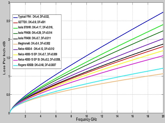
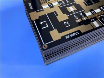
Rogers 4350B PCB vs Megtron 6 PCB PCBs are evolving with the continually increasing demands of the electronics and telecom market. We are sitting on the eve of widespread deployment of 5G wireless technology across the globe. This will mean that the underlying electronic devices (primarily cell phones and other network-dependent electronics) will need to cope with the high-frequency demands of the 5G technology. When it comes to high-frequency circuits, the most commonly used PCB material, FR-4, doesn’t seem to cut it. FR-4, while being widely used, tends to be a very loss-generating material in high-frequency circuits. For such circuits, specialized materials (laminates) are chosen. There is a wide variety of them available in the market, from season manufacturers like Isola, Itera, Taconic, Rogers, and Panasonic. Among them, two of the most commonly used materials are Rogers R04350B and Panasonic Megtron 6. Let’s see the difference between the two. Similarities between Rogers 4350B and Panasonic Megtron 6 Finding the low-loss material that will provide the best balance of performance and board cost for a given application is morecomplicated than simply comparing laminate datasheets and prices. Datasheets do not reveal which materials involve relativelymore or unusual processing steps during PCB fabrication, which can raise manufacturing cost. Consider Rogers 4350B and Panasonic Megtron 6, which have similar low Df and Dk values, have been used extensively in RF applications, and areincreasingly being used for high-speed digital products.Both are based on hydrocarbon resins; the Rogers resin has a ceramicfi ller. Neither laminate is available clad with quarter-ounce copper. The thinnest foil available for the Rogers material is half-ounce,and for Megtron 6, one-third-ounce.Both materials are available with low-profi le foils to prevent signal refl ections at highfrequencies. Both Rogers 4350B and Megtron 6 are specifically designed high-speed laminates. Both fall into the extremely low-loss category of laminates (if considered based on the loss). In terms of highest efficiency and least incurring losses, Rogers 4350B and Megtron 6 are second only to specifically designed extremely low loss, microwave laminates like Taconic RF-35TC. Both the materials are very similar when it comes to many electrical and transmission characteristics. Take the signal loss, for example. Megtron 6 tends to be the superior material for frequencies below 5, but over that, Rogers 4350B has a slight edge (just a shade better than Megtron 6). If we dive a bit deeper into the laminate material’s electrical performance properties, two other terms that you might have heard are Permittivity (Dk) and Loss tangent (Df). Megtron 6 has a Dk of 3.7 and Df of 0.002 at 2 GHz (3.3 and 0.004 at 10 GHz). Whereas Rogers 4350 has a Dk of 3.43 and Df of 0.0037 at 10 GHz. So in higher frequencies, Rogers 4350B has a bit of an edge in these commonly compared electrical characteristic...
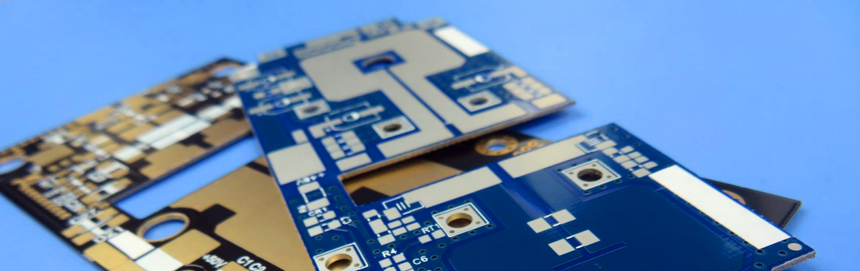
High-Quality PCB Material That Meets Your Needs PBC specs and costs for printed circuit board prototyping and production vary depending on the PCB materials used. There are 1 or 2 layer boards that just need one pre-preg "core" and multiple layer boards that are constructed using two or more core types. Depending on the intended purpose and the needed thickness, pre-preg, a material comprised of thin layers of fiberglass "pre-impregnated" with a bonding agent or metal core in a sheet shape, comes in a variety of sizes. Your board's thickness can range from a few mils for flex boards to a quarter inch for hefty burn-in boards. Core materials resemble slim double-sided boards with dielectric materials such as fiberglass along with a copper foil placed on each side; these usually come in predefined thicknesses. PCB Prototype using FR4 A glass fiber epoxy laminate is the most popular family of substrates for printed circuit boards, or FR4. The most common material is FR4, but higher numbers (such FR4-06 and FR4-08) have lower dielectric constants and greater temperature coefficients. As you advance through the family, the temperature rises, with FR4 having a beginning Tg of 140 degrees Celsius and FR4-06 having a Tg of 170 degrees. PCB Prototype using Metal Core Metal Core is well-liked in printed circuit boards for light-emitting diodes because it is excellent at removing heat. A single layer MCPBC consists of a copper circuit layer, IC components, a solder mask, an aluminum and non-conduction layer, and a copper circuit layer. To assure the safety of the LEDs, the metal core works as an incredible heat sink. PCB Prototype Using Polyimide for Flexibility Polyimide is more durable than FR4 and can withstand higher temperatures, which makes it perfect for use in electrical insulation applications that adhere to class H standards. The polyimide is made up of a silicone adhesive structure and a thermoresistant polyimide layer. Edge connectors, gold edge fingers used in wave soldering, and reflow soldering methods used in PCB assembly are all safeguarded by it. The hue of polyimide is another intriguing characteristic. The majority of boards are produced in green, but polyimide is easily distinguished by its brown hue. PCB Prototype Using Teflon for High Frequency Base: PTFE/Woven glass Because Teflon is softer than FR4, PCB materials need special drilling. The idea that certain materials are exotic is no longer associated with them. A material that is readily available and has a track record of performance, PTFE/woven glass base materials enable both the rapid expansion of application operations and the fulfillment of high-frequency demands. PCB Prototype Using Arlon for Longer Life at Higher Temperatures For the PCB fabrication of high performance and frequency-dependent printed circuit manufacturing, use Arlon materials. Applications with large lifespan temperatures and lead-free soldering are two examples of common applications that are susceptible t...
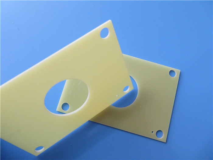
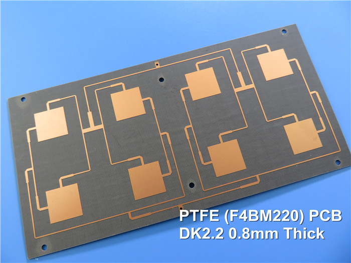
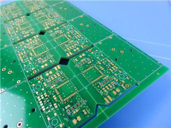
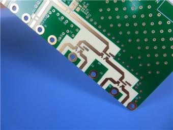
BASE MATERIALS OF PCB The insulation, material makeup, and fire-retardant properties of the base materials are frequently used to classify substrates. Bakelite, fiberglass, and various plastics are common PCB base materials. Manufacturers of PCB substrates typically combine insulating prepreg materials made of glass-fiber non-woven material and epoxy resin laminated to copper foil to create copper foil substrates. The common types of PCB substrates are as follows : FR-4: Fiberglass + Epoxy Resin. This is the most common type of PCB substrate. As Tg is only about 130°C, the High Tg FR-4 is recommended for products requiring processing or operating at high temperatures. High Tg FR-4: Fiberglass + Epoxy Resin. This is the second common type of PCB substrates after the FR-4 PCB substrates with a glass transition temperature (Tg) over 150°C is called High Tg substrates. CEM-1: Fiberglass Fabric + Epoxy Resin coated on cotton. CEM-3: Fiberglass Fabric + Epoxy Resin coated on fiberglass non-woven fabrics. Ceramic PCB: Powder Ceramics + Fiberglass Teflon PCB: Teflon + Fiberglass Surface treatment of PCB: Due to the PCB's copper surface's propensity for oxidization in the presence of oxygen, exposed regions that aren't covered by the solder mask are given a surface coating to prevent oxidation. Surface finishes of diverse materials, costs, and protection capabilities are produced to fulfill the requirements of various ways of post-processing. These are the typical PCB surface finishes: Surface treatments include immersion silver, gold plating, HAL, LF-HASL, ENIG, and bare copper. To examine a comparison of several PCB surface finishes.
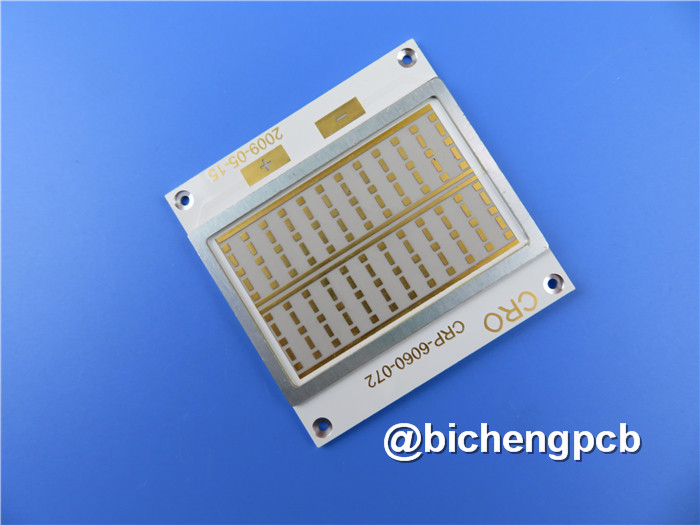
What is the base material of a metal core PCB? Metal-core PCB commonly use aluminum-based, iron-based (including silicon steel), copper-based, and CIC as the base substrate. 1.Aluminum-based substrate The most commonly used aluminum-based substrates for manufacturing metal-core PCBs are LF, L4M, and LY12, which require a tensile strength of 294N / mm. The elongation is 5%, and the thicknesses generally used are four specifications of 1mm, 1.6mm, 2mm, and 3.2mm. Generally, the thickness of the aluminum layer commonly used in the aluminum-based PCB used for communication power is 140um, and copper foil is attached above and below. 2. Copper-based substrate The commonly used copper-based substrates have a tensile strength of 245 to 313.6 N / mm2, an elongation of 12%, and generally five thicknesses of 1 mm, 1.6 mm, 2 mm, 2.36 mm, and 3.2 mm. 3.Iron-based substrate Generally used in production are cold-rolled rolled steel plates, which are low-carbon steels with thicknesses of 1mm and 2.3mm, or phosphorus-containing iron-based thicknesses of 0.5mm, 0.8mm, and 1.0mm. 4. Features of metal core PCB Heat dissipation Conventional PCB substrates are generally poor thermal conductors, and the heat dissipation from the interlayer insulation material is very slow. The internal heat of various electronic equipment and power equipment cannot be eliminated in time, resulting in high-speed component failure. The metal core PCB has good heat dissipation. The metal core has large thermal capacity and high thermal conductivity, which can quickly dissipate the heat inside the board. If the metal core is connected to the case and the external heat sink, the heat dissipation effect is better. Because electronic equipment and communication systems use metal-core PCBs, the fans in the equipment can be eliminated, the size of the equipment is greatly reduced, and the efficiency is improved, which is especially suitable for electronic equipment with closed chassis. Thermal expansion Thermal expansion and contraction are the common characteristics of materials, and the thermal expansion coefficients of different materials are different. PCB is a composite material composed of resin, reinforcing material, and copper foil. Its thermal expansion coefficient is anisotropic. In the XY axis direction, the thermal expansion coefficient CTE of PCB is 13 × 10-6 ~ 18 × 10-6 / ℃. The thickness direction (Z-axis direction) is 80 × 10-6 to 90 × 10-6 / ° C, the CTE of copper is 16.8 × 10⁻⁶ / ° C, and the CTE of the sheet-shaped ceramic body is 6 × 10⁻⁶ / ° C. From these data, it can be seen that the CTE of the metalized hole wall of the PCB and the connected insulating substrate in the z-axis is very different. If the heat generated cannot be eliminated in time, thermal expansion and contraction will easily cause the metalized hole wall plating to crack or disconnect. When soldering a ceramic chip carrier device on a PCB, due to the difference between the device and the PCB material CTE,...
What is the difference between PCB and metal core PCB? One important difference to understand between metal core PCB and standard PCB is how the materials work together to create the necessary result. In metal core PCB, there is a single layer of copper with is bonded to a layer of conductive dielectric material, which is further bonded to a thick metal layer (typically Aluminum 5052, Aluminum 6061, or Copper C1100). The dielectric used is approximately 6-7 times as thermally conductive as FR4. The dielectric is to be kept as thin as possible. This reduces the distance from the heat source to the metal plate which is more conductive than the dielectric. As you know, the metal plate on the bottom side is the thickest element in the structure. It is available in several different thicknesses, however, there are three most common thickness, such as 1.0mm, 1.5mm, and 3.2mm as they are the easiest to purchase. The metal also gives the PCB rigidity and does not require any surface finish or solder mask. FR-4 PCB Vs. Metal core PCB comparison Plated through holes: in general, plated through holes are used in FR-4 PCB. It can be through hole components if required. In metal core PCB, plated through holes are not available for 1-layer PCB. All components are surface-mounted. Conductivity: FR-4 PCB has low thermal conductivity, in general about 0.3W, however, MCPCB has a higher thermal conductivity between 1.0W and 4.0W, most commonly about 2.0W. Thickness: FR-4 PCB has a wide range of thickness, also uses many material combinations and layers. Metal core PCB has a limited thickness variation. Thermal relief: as usual, Thermal relief in FR4 PCB involves vias for heat transfer. And it has a longer drilling processing cycle. Metal core PCBs don’t require via as their own thermal dissipation. Consequently, they do not require drilling, deposition and plating processes. Solder mask: FR-4 PCB solder mask is dark colors such as green, red, black and so on, which usually applied on top and bottom. For LED boards, metal core PCB solder mask are almost exclusively white and they are only applied to the top. Machining process: FR-4 PCB uses standard processing such as drilling, routing, v-scoring, countersink, counterbore and so on. whereas in metal core PCBs, there is a distinctive difference in the v-scoring process i.e. diamond-coated saw blades are used for the added strain from cutting into metal.
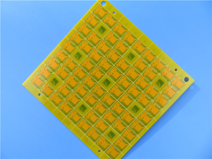
What Makes the HDI PCB Different? The advantages of HDI PCBs over ordinary PCBs are listed below, demonstrating how they differ from other kinds of PCBs. 1. Enhanced Thermal Efficiency Due to the use of copper foil rather than aluminum foil in FR4s, HDI PCBs have higher thermal performance. In comparison to aluminum, copper is a far superior heat conductor and can dissipate heat much more effectively. Less power is wasted as a result, which is crucial when working with high-power circuits like motor drivers or power supplies. 2. Improved Signal Integrity Because signal traces from multiple layers can be routed closer together on the same plane, HDI pcb boards are able to retain signal integrity over longer distances than conventional single-layer boards. Additionally, due to capacitance effects, signal traces on one layer can be routed over other traces on another without degrading the quality of the signal. 3. Increasing Reliability By enhancing the insulation between conductors and circuits, lowering crosstalk, and preventing short circuits between signals moving on neighboring planes, HDI pcb boards improve system dependability. Additionally, they improve mechanical strength by lowering stress concentrations brought on by densely packed components in high numbers. 4. Greater Density Compared to conventional single-layer boards, HDI pcb boards support more electrical connections per unit space. The usage of several layers in the stackup and blind vias as layer interconnects are mostly to blame for this. 5. More Compact Size HDI PCBs are more compact than conventional PCBs because of the enhanced trace density. As a result, they take up less space on one board, making them perfect for portable gadgets like laptops, tablets, and smartphones. Additionally, because of their reduced size, they are simpler to manufacture on a single assembly line without the need for special tools for each product's various sizes. 6. Mechanical Power Standard PCBs cannot sustain the amount of stress that HDI PCBs. This is a result of their construction, which consists of several sheets of thin plastic linked together with an epoxy adhesive. Depending on the kind of resin used in construction, each layer's strength varies. 7. Lower Price HDI pcb boards can be less expensive than other kinds of multilayer boards and other kinds of boards produced from copper-clad laminate because they are easier to make and less expensive to create than single-sided boards (CCL). Both low-volume production runs and high-volume production runs are compatible with them. HDI PCBs for a Variety of Applications Where reliability is crucial, HDI PCBs are frequently utilized in avionics, military, and aerospace applications. A typical airplane requires hundreds of microcircuits, sensors, and other electronic parts, all of which must be wired together. The conventional method calls for all of these wires to be soldered directly on top of one another, which frequently results in a number of iss...
Categories
New Products
Wangling 5mil 0.127mm TFA300 Core 2-layer Immersion Gold Green Solder Mask PCB
7.5mil AGC Taconic TLY-5 Substrate Custom PCB EPIG Finish Bare Copper
10mil Rogers CuClad 250 Immersion Gold 2-Layer Rigid Microwave PCB
20mil F4BTMS450 Wangling DK4.5 Laminate Custom PCB HASL LF Finsh
F4BME275 Wangling DK2.75 Laminate 2-Layer 1.6mm Pure Gold RF Custom PCB
Wangling F4BTD350S High Frequency PCB 2-layer 20mil Thick ENIG DK3.5 Substrate
12-layer TG200 TU-872 SLK High-Speed FR4 1.68mm PCB with ENIG Impedance Control
12-Layer RO4350B + RO3010 3.14mm Hybrid PCB Nickel-Free EPIG Surface Finish Blind Via
 6-11C Shidai Jingyuan, Fuyong, Baoan, Shenzhen, Guangdong, China 518103


For inquiries about our products or pricelist, please leave to us and we will be in touch within 24 hours.
© Copyright: 2026 Shenzhen Bicheng Electronics Technology Co., Ltd.. All Rights Reserved.

IPv6 network supported


