
 Call Us Now !
Tel : +86 755 27374946
Call Us Now !
Tel : +86 755 27374946
 Order Online Now !
Email : info@bichengpcb.com
Order Online Now !
Email : info@bichengpcb.com
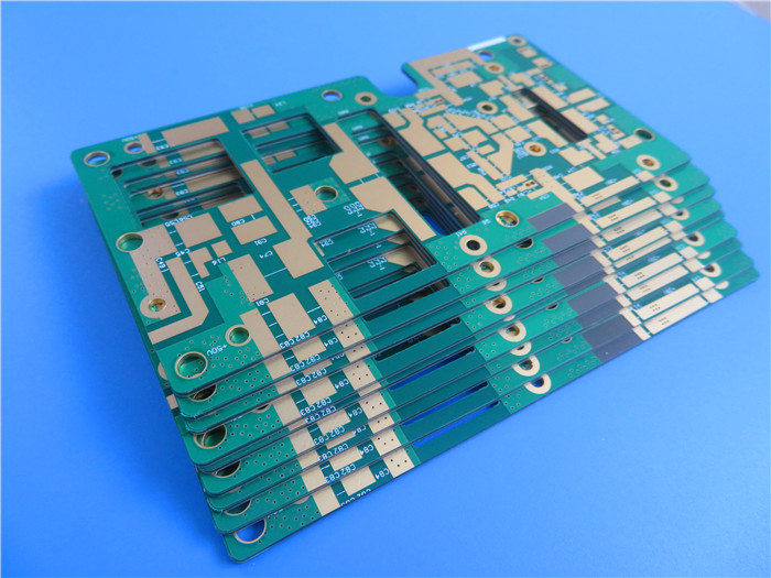
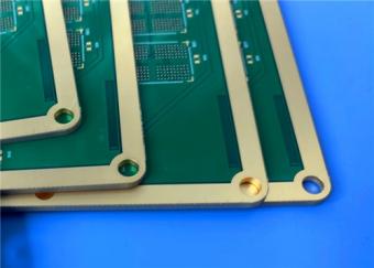
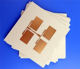
Rogers TMM Series PCB: TMM 3, TMM 4, TMM 6, and TMM 10 Rogers TMM thermoset microwave materials are composites of hydrocarbon ceramics and thermoset polymers designed specifically for strip-line and microstrip applications. TMM is available in a variety of claddings and dielectric constants. TMM laminates have mechanical and electrical properties that make them suitable for a variety of applications. TMM has a very good thermal expansion coefficient, a slow thermal change of the dielectric constant (Dk), and a stable dielectric constant. Greater copper coating specifications are available from TMM. These laminates possess the qualities of both ceramic and PTFE microwave circuit laminates without requiring the manufacturing processes for those materials. TMM is distinct from other laminates in that it does not require sodium napthanate treatment prior to electroless plating. TMM laminates have an extremely low thermal coefficient of Dk, which is usually less than 30 ppm/°C, which is one of their most amazing properties. TMM laminates are based on thermoset resins, and do not soften when heated. As a result, wire bonding of component leads to circuit traces can be performed without concerns of pad lifting or substrate deformation. TMM laminates combine many of the desirable features of ceramic substrates with the ease of soft substrate processing techniques. Substrate thicknesses of 0.015” to 0.500” are available. The base substrate is resistant to etchants and solvents used in printed circuit production. Consequently, all common PWB processes can be used to produce TMM thermoset microwave materials The Benefits of Rogers TMM TMM laminates from Rogers are high-quality microwave materials with excellent electrical and mechanical properties. These materials bring together the advantages of PTFE microwave circuits and ceramic laminates. Rogers TMM laminates have exceptional mechanical properties because they resist cold and creep flow, making them mechanically reliable and stable. Chemical reagent resistance: Rogers TMM laminates are chemical reagent resistant, which helps to ensure that there is no damage during the placement and production process. After being exposed to chemical reagents for a set period of time, these microwave materials retain their original properties. Rogers TMM laminates are made of thermosetting resin, which ensures good wire bonding. These materials can withstand any temperature, including extreme heat. Absorption of moisture: These laminates can endure in a humid setting. Rogers TMM is a good material for a setting with high levels of humidity because it can absorb moisture from its surroundings. The laminate known as Rogers TMM is made of ceramics, hydrocarbons, and thermosetting polymers. Comparing these laminates to some alumina filler substrates reveals processing advantages. Rogers TMM laminates come in a variety of thicknesses, including TMM 10, TMM 6, TMM 4, etc., but they all share a number of characteristics. The m...
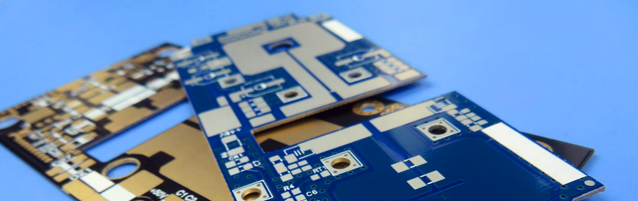
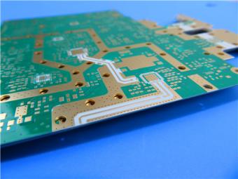
Today, a wide range of portable wireless and commerce sectors, including health, communication, etc., have adopted Microwave PCB technologies. Circuit interferences and radiation in the PCB design are difficult to control because microwave circuit boards are distributed variable circuits that continue to produce skin effects and interaction effects. The most common issues include resonance issues caused by absurd layouts, cross-interference between digital and analog circuitry, power interference with noise, and related resonance issues. As a result, it is crucial for Microwave PCB design to weigh the advantages and disadvantages of PCB design and make an effort to cut down on interference. What is the Microwave PCB? The RF and microwave PCB boards are distinctive and cutting-edge PCB kinds created to operate at signal frequencies between megahertz and gigahertz (medium frequency to extremely high frequency). From cellphones to military radars for network transmissions, these frequencies are used everywhere. Extremely specific materials and technology are required for this PCB equipment, which are not readily available from many producers. How do RF and Microwave PCB differ? The radiofrequency of RF circuit boards and microwave PCBs is their primary differentiator. Microwave PCBs are categorized as RF circuit boards that operate over 2GHz. Microwave PCBs and RF circuit boards are used for networking signals in any application that calls for the reception and transmission of radio signals. Radar stations and mobile phones, for instance, are two common applications. Microwave PCB advantages: Since electronics are so useful, this technology is becoming more and more popular every day. The PCB design for microwaves has several benefits. Let's look at them now. High Stability: Extreme temperature PCB design is especially stable. When analog applications are used, these PCBs are capable of operating at 40 GHz. High Speed: Signals can pass through the PCB more quickly and imperturbably thanks to the low tangent and consistency of the loss. Components: Fine pitch components can be successfully mounted on the board without too many issues. Costs reduced: In order to reduce PCB assembly costs while maintaining optimal PCB performance, the materials may be combined in a panel storage system. Multifaceted: A PCB engineer can quickly align several layers of boards into complex patterns because to the usage of low CTE components. Microwave PCB Materials: Conductivity constant (DK), overindulgence feature, thermal expansion coefficient (CTE), dielectric constants, and current conductivity are important factors that determine laminate circuit performance for microwave/RF printed circuit boards when designing PCB components at higher frequencies. The most identifiable different frequencies material for PCB cover workers is polytetrafluoroethylene (PTFE). It is a manufactured thermoplastic fluoropolymer with good radio wave dielectric properties. Here is a brief s...

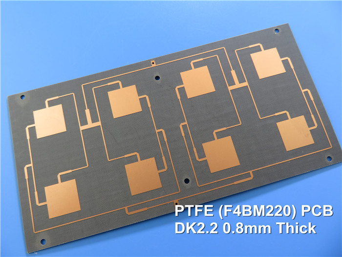
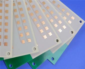
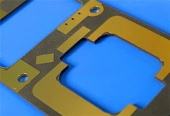
Teflon PTFE PCB Characteristics Polytetrafluoroethylene, also known as Teflon PCB or PTFE, is a chemical compound that is commonly referred to as "non stick coating" or "easy to clean substance." This substance is nearly insoluble in all solvents and exhibits acid resistance, alkali resistance, and resistance to different organic solvents. Teflon can be utilized as an appropriate coating for high-end electronic devices' PCB proofing as well as for easy cleaning of the inner layer of water pipes due to its high temperature resistance and extremely low friction coefficient. This is another another typical component used to make PCBs. Teflon is a strong and lightweight substance. This substance is frequently used in applications that demand precise limits. At high temperatures, Teflon won't expand. This substance's flame retardant properties are one of its benefits. It is ideal for high-speed applications because of the characteristics of this material. Teflon is durable and maintains a stable temperature.. Teflon PCB exhibits a number of outstanding qualities. Making Teflon PCB examples begins with the choice of materials. Teflon PCB is used in the Wangling F4B, Rogers 5 series, and Rogers 3 series. Prototyping of flexible PCBs frequently involves the use of plastics. A handy material for making PCBs is PTFE. Teflon PCB provides several special benefits. Function test: Following the creation of the Teflon PCB sample, the board successfully passes the test to access its functions as intended. Teflon circuit boards can tolerate extremely cold and hot temperatures. It is employed in military and aerospace applications primarily for this reason. The plate can function between - 270 and 315 °F and between -454 and 600 °F. It can withstand any temperature and prevent cracking. High dielectric strength: due to the high dielectric strength of the plate, it does not conduct electricity. It works perfectly as an insulator. The insulating power of this material can protect the equipment from electric breakdown. Durability: PTFE PCB is an ideal choice because it is very durable. It can withstand oxidation, UV, embrittlement or discoloration. Because of its durability, it is a cost-effective option. Mechanical rigidity: Teflon PCB has mechanical stability. This makes it ideal for applications exposed to high levels of mechanical stability. Teflon PCB has good thermal conductivity. High temperature resistance: long-term use temperature: 200~260 ℃; Low temperature resistance: soft at - 100 ℃; Corrosion resistance: resistant to aqua regia and all organic solvents; Weather resistance: the best aging life of plastics; High lubrication: it has the minimum friction coefficient (0.04) among plastics; Non sticky: it has the minimum surface tension among solid materials without adhering to any substance; Physiological inertia: With excellent electrical performance, it is an ideal class C insulating material. A thick layer of newspaper can block 1500V high voltage; ...
Overview of Global PCB Printed Circuit Board Market ① PCB global market space is vast The PCB industry is the industry with the largest output value among the global electronic component subdivision industries. In 2017 and 2018, the global PCB output value grew rapidly, with an increase of 8.6% and 6.0% respectively. Due to the weak macroeconomic performance and the impact of the Sino-US trade war, the global PCB output value in 2019 decreased by 1.7% compared with the previous year. Affected by the prevention and control of the new crown epidemic in 2020, scenarios such as home office and home study will stimulate demand for personal computers, consumer electronics, and network communications, and the gradual recovery of automobile production and demand in the second half of 2020 will drive PCB demand to pick up. According to Prismark statistics, the total output value of the global PCB industry in 2021 will be US$80.92 billion, an increase of 24.1% over 2020. Driven by factors such as intelligence and low carbonization, PCB downstream application industries such as 5G communications, cloud computing, smart phones, smart cars, and new energy vehicles are expected to flourish, and the vigorous development of downstream application industries will drive continued growth in PCB demand . According to Prismark's forecast, the total output value of the global PCB industry will grow by 4.2% in 2022; the global PCB market will maintain moderate growth in the next five years, with a compound annual growth rate of 4.6% from 2021 to 2026. ②The global PCB industry is shifting to Asia, especially mainland China The PCB industry is widely distributed around the world. The developed countries in the United States, Europe and Japan started early, developed and fully utilized advanced technical equipment, and the PCB industry has made great progress. Before 2000, the three major regions of America, Europe and Japan accounted for more than 70% of the output value of global PCB production and were the most important production bases. In the past two decades, relying on the advantages of Asia, especially mainland China, in labor, resources, policies, and industrial agglomeration, the global electronics manufacturing capacity has been transferred to mainland China and other Asian regions. With the transfer of the global industrial center to Asia, the PCB industry presents a new pattern with Asia, especially mainland China as the manufacturing center. Since 2006, mainland China has surpassed Japan to become the world's largest PCB production region, and the output and value of PCB rank first in the world. As the largest production area in the global PCB industry, mainland China has accounted for 54.6% of the global PCB output value from 8.1% in 2000 to 54.6% in 2021. The PCB industry in regions and other places has developed rapidly. ③Development trend According to Prismark's prediction, Asia will continue to dominate the development of the global PCB market in the n...
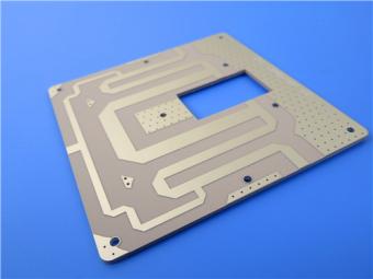
What is Rogers PCB? Rogers PCB is a type of high-frequency board that raw material is produced by Rogers company. Epoxy resin distinguishes it from traditional PCB boards (FR4). It uses a ceramic base as the high-frequency material and lacks a glass fiber in the middle. The thermal stability and dielectric constant of Rogers are superior. It can be utilized to address the shortcomings of PTFE substrates since copper foil and its dielectric constant thermal expansion coefficient have very similar properties. It is excellent for commercial microwave, radio frequency, and high-speed electronic design applications. Due to its low water absorption, it is perfect for high-humidity applications, giving clients in the high-frequency board sector access to the best raw materials and resources that fundamentally improve the quality of the finished product. Once they are aware of FR4's subpar performance at microwave frequencies, many PCB designers see Rogers as a need for high-frequency PCB materials. PCBs using the Rogers laminates are called Rogers PCB. A company called Rogers creates laminate materials that are utilized to create PCBs. PCBs are often constructed using the FR4 material, which is a glass fiber and epoxy resin hybrid. The FR4 laminates that Rogers supplies have stronger high-frequency characteristics. The primary materials they offer have high-frequency characteristics similar to Teflon. Rogers offers a wide variety of materials used for high-frequency PCBs with a relative permittivity ranging from 2.3 to 10.2 and low dielectric losses: Fluoroplastics RT/duroid series (RT500, RT600); Reinforced fluoroplastics RO3000 and RO4000 series; Hydrocarbon ceramics TMM; Reinforced laminates ULTRALAM 2000. All materials have a standard range of thicknesses and can have one- or two-sided metallization from electrodeposited or rolled foil (copper, brass, aluminum) of a given thickness. Rogers materials can be combined with FR4 to create printed circuit boards because they both have high properties (loss tangent, dielectric constant, etc.). The following beneficial qualities are offered by Rogers PCBs: Throughout the performance, they have the least amount of electrical signal loss. They also have the lowest dielectric losses. They offer efficient thermal function management. They have a wide variety of dielectric constant values. They offer the minimal outgassing capability, which is crucial for applications in space. Additionally, they feature effective impedance control. The ceramic hydrocarbon lamination of the Rogers PCBs is combined with an insulating dielectric layer. For electrical connections and changes, this layer functions as a poor conductor. In this case, good insulating materials include the oxides of metals and other substances like mica and porcelain. The special qualities of the insulating substance are enhanced by this use. This insulating layer significantly lowers the loss of signals on PCBs. Additionally, it aids in preserving the ...
Categories
New Products
2-Layer 20mil FSD1020T ENIG High-Frequency PCB with Via Resin Plugged and Capped
4-Layer F4BM265+S1000-2M Material Hyrbid PCB with Blind Via Impedance Control & ENIG
4-Layer Wangling WL-CT338 + FR4 Hybrid PCB ENIG Green Solder Mask White Silkscreen
6-layer Isola 370HR High-Tg FR-4 PCB 2μ" ENIG Impedance Controlled
6-Layer RO4003C + FR4 Mixed Dielectric PCB with Hard Gold Plating Blind Via
30mil Taconic CER-10 2-layer Immersion Silver DK10 High Frequency Laminate PCB
31mil Rogers RT/duroid 5880 Double-sided Bare Copper ENIG Finished PCB
Wangling TFA294 Laminate 40mil Immersion Silver No Solder Mask Silkscreen Custom PCB
 6-11C Shidai Jingyuan, Fuyong, Baoan, Shenzhen, Guangdong, China 518103


For inquiries about our products or pricelist, please leave to us and we will be in touch within 24 hours.
© Copyright: 2026 Shenzhen Bicheng Electronics Technology Co., Ltd.. All Rights Reserved.

IPv6 network supported


