

 Call Us Now !
Tel : +86 755 27374946
Call Us Now !
Tel : +86 755 27374946
 Order Online Now !
Email : info@bichengpcb.com
Order Online Now !
Email : info@bichengpcb.com
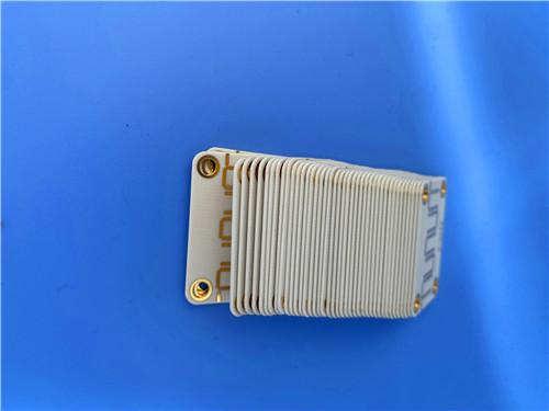
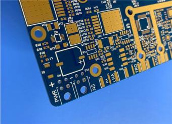
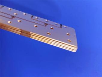
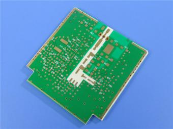
This AD300D double-sided PCB represents a convergence of advanced material science and precision manufacturing.
Item NO.:
BIC-532-v617.0Order(MOQ):
1-10Payment:
T/TProduct Origin:
ChinaShipping Port:
ShenzhenLead Time:
7-10 days
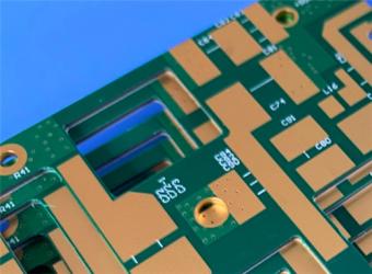
Rogers AD300D 2-layer 40mil 1.016 mm EPIG Bare Copper High Frequency PCB
Product Overview
Designed for high-performance wireless and RF communication applications, the AD300D 2-layer 40mil EPIG PCB is a precision-engineered solution built to meet IPC-Class-2 quality standards, combining premium PTFE-based substrate performance with strict manufacturing tolerances and reliable surface finishing.
As a specialized RF-focused PCB, this product is optimized for low signal loss, consistent dielectric properties, and exceptional passive intermodulation (PIM) performance, addressing the core demands of modern wireless antenna systems, cellular infrastructure, and automotive telematics. Unlike standard commercial PCBs, this unit leverages AD300D ceramic-filled, glass-reinforced PTFE laminate material to deliver stable electrical performance across wide frequency and temperature ranges, with zero compromise on mechanical durability and manufacturing repeatability. Every unit undergoes 100% full electrical testing prior to global shipment, ensuring full compliance with customer design files and operational reliability in critical communication environments.
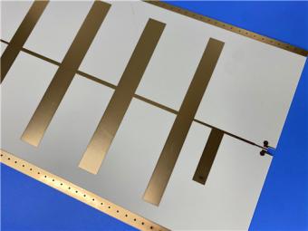
1.PCB Construction Overview
This section outlines the core physical and manufacturing parameters of the PCB, defining material selection, dimensional tolerances, conductive properties, and finishing specifications to confirm compatibility with standard RF assembly processes and strict quality benchmarks.
|
Parameter |
Specification |
|
Base Material |
AD300D (Ceramic-filled PTFE) |
|
Layer Count |
2 (Double Sided) |
|
Board Dimensions |
67 mm x 102.6 mm per piece (Tolerance: +/- 0.15 mm) |
|
Minimum Trace/Space |
4 mils / 6 mils |
|
Minimum Hole Size |
0.4 mm |
|
Blind/Buried Vias |
None |
|
Finished Board Thickness |
1.2 mm (0.047") |
|
Finished Copper Weight |
1 oz (35 μm / 1.4 mils) on both outer layers |
|
Via Plating Thickness |
20 μm (in hole) |
|
Surface Finish |
EPIG (Electroless Palladium Immersion Gold) - Nickel Free |
|
Top Silkscreen |
No |
|
Bottom Silkscreen |
No |
|
Top Solder Mask |
No |
|
Bottom Solder Mask |
No |
|
Electrical Test |
100% tested prior to shipment |
2. PCB Stackup
The 2-layer stackup is engineered for balanced electrical performance and mechanical stability, using a thick 40mil AD300D core with consistent 35μm copper foils on both outer layers to minimize signal distortion and ensure uniform dielectric distribution for RF applications.
|
Layer |
Material |
Thickness |
|
Layer 1 (Top) |
Copper Foil |
35 μm (1 oz) |
|
Core |
AD300D (PTFE/Ceramic) |
1.016 mm (40 mil) |
|
Layer 2 (Bottom) |
Copper Foil |
35 μm (1 oz) |
3. PCB Statistics
This compact, low-component-count layout is optimized for dedicated RF antenna functions, featuring a minimal net count and targeted pad/via configuration to reduce signal interference and streamline assembly for specialized wireless communication modules.
|
Category |
Count |
|
Components |
15 |
|
Total Pads |
41 |
|
Thru Hole Pads |
29 |
|
Top SMT Pads |
12 |
|
Bottom SMT Pads |
0 |
|
Vias |
36 |
|
Nets |
2 |
4. Artwork, Quality, and Availability
To ensure a seamless transition from design to production, the following standards and logistics apply to this product:

5. Introduction to AD300D Material
The foundation of this Rogers PCB's superior performance is the AD300D laminate. This material is a ceramic-filled, glass-reinforced PTFE composite specifically developed to meet the stringent requirements of the modern wireless antenna market. Its formulation is designed to provide a controlled dielectric constant, exceptionally low signal loss, and industry-leading Passive Intermodulation (PIM) performance. Importantly, it is compatible with standard PTFE fabrication processes, offering a cost-effective path to enhanced electrical and mechanical stability in demanding RF environments.
6. Key Features
1)Controlled Dielectric Constant: DK of 2.94±0.05 at 10 GHz / 23°C, ensuring repeatable and predictable circuit performance.
2)Low Dissipation Factor: Df of 0.0021 at 10 GHz / 23°C, minimizing signal loss for high-efficiency power transfer.
3)Stable Thermal Expansion: CTE of 24 ppm/°C (X), 23 ppm/°C (Y), and 98 ppm/°C (Z) from -55 to 288°C, providing excellent plated through-hole (PTH) reliability.
4)Consistent Electrical Properties: Thermal coefficient of DK measured at -73 ppm/°C, ensuring stable performance across temperature fluctuations.
5)Flame Retardant: UL 94 V-0 rated for safety compliance.
7. Benefits
1)Superior Signal Integrity: The ultra-low loss tangent (<0.002 at 10 GHz) guarantees excellent circuit performance across all typical wireless frequency bands, from cellular to automotive telematics.
2)Enhanced Antenna Performance: The very low PIM rating (-159 dBc at 30 mil, 1900 MHz) is critical for high-performance antenna systems, significantly reducing yield loss due to PIM-related issues and ensuring cleaner signal transmission.
3)Manufacturing Reliability: Excellent dimensional stability translates directly to repeatable circuit performance and higher manufacturing yields, reducing costs and lead times.
4)Lead-Free & Reliable: The EPIG surface finish provides a flat, solderable surface without the use of magnetic nickel, preserving signal integrity and meeting modern environmental standards.
8. Typical Applications
This AD300D high frequency PCB is ideally suited for a range of high-frequency applications where material performance is critical to overall system success:
In summary, this AD300D double-sided PCB represents a convergence of advanced material science and precision manufacturing. It is designed not just to function, but to excel in the most challenging RF environments, providing our customers with a reliable, high-performance foundation for their critical technologies.


Previous:
Rogers Kappa 438 PCB 2-Layer 30mil 0.762mm Laminate ENIG Bare Copper SurfaceNext:
50mil RF-60A Laminate Custom PCB double-sided Pure Gold Plating Bare CopperIf you have questions or suggestions,please leave us a message,we will reply you as soon as we can!
Categories
New Products
20-Layer Panasonic TU872 HDI PCB ENEPIG 3.0mm Finished Thick Laser-drilled Blind Vias
10-Layer Rogers RO4003C + 370HR FR4 Hybrid Laminate PCB ENIG Impedance Control
8-Layer 10oz Heavy Copper TU-865 Substrate PCB With ENIG Blind &Buried Via
4-Layer Rogers RO3210 + RO4450F PCB ISIG Surface Finish 1.321mm With Blind Via
4-Layer Rogers RO3003+TG170 FR-4 Hybrid PCB Immersion Silver Green Solder Mask
WL-CT440 PCB 30mil 0.762mm Wangling Laminate ENIG Finish No Solder Mask
TP1600 PCB 31.49mil High DK16 Wangling Laminate Pure Gold Plating
TLX-9 PCB 10mil 0.254mm Taconic High Frequency Laminate EPIG Nickle-free

RF-10 25mil Taconic PCB Materials stands out as a high-performance solution for RF applications. Its exceptional electrical properties, dimensional stability, thermal conductivity, and adhesion characteristics make it an ideal choice for demanding applications.
The PCB has a 4-layer hybrid stackup with a 0.5oz+plating ground layer, two 1oz ground layers, and a 0.5oz+plating signal layer.
The dimensions of the board are 55.00 x 26.00 mm, with a tolerance of +/- 0.15mm. The board has 16 components, 26 total pads, 9 through-hole pads, 10 top SMT pads, 7 bottom SMT pads, 77 vias, and 82 nets.
Rogers RO4003C PCB is an innovative and advanced circuit board that is made with high-quality materials.
The RO4350B PCB offers a range of benefits that make it an ideal choice for high-frequency applications. Its low dielectric loss and high thermal conductivity make it perfect for high-frequency applications such as RF and microwave circuits.
Bicheng PCB Ships High-Quality PCBs with Shengyi Tg150 ℃ S1000H Material and Advanced Stackup
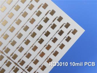
Rogers RO3010 PCB is ideal for a wide range of high-frequency applications, including power amplifiers, filters, couplers, and antennas.
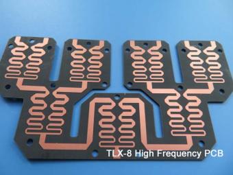
TLX-8 features low dielectric loss, low moisture absorption, and excellent thermal stability, making it ideal for high-frequency and high-speed applications. It has a low dissipation factor, which helps to minimize signal loss and distortion.
 6-11C Shidai Jingyuan, Fuyong, Baoan, Shenzhen, Guangdong, China 518103


For inquiries about our products or pricelist, please leave to us and we will be in touch within 24 hours.
© Copyright: 2026 Shenzhen Bicheng Electronics Technology Co., Ltd.. All Rights Reserved.

IPv6 network supported


