
 Call Us Now !
Tel : +86 755 27374946
 Order Online Now !
Email : info@bichengpcb.com
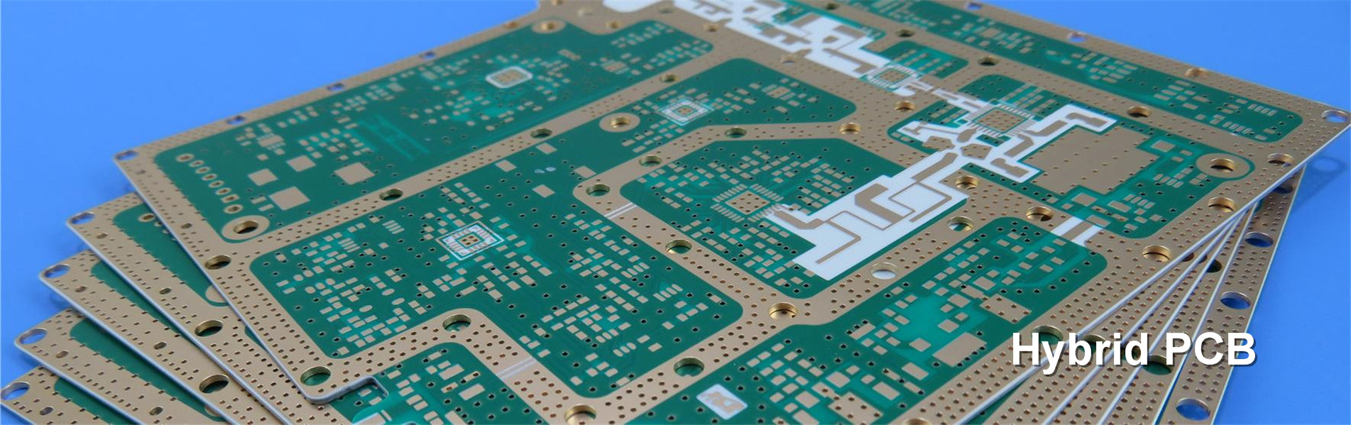
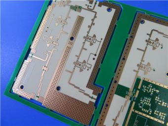
This 4-layer RO4003C FR-4 hybrid PCB is a cost-engineered RF platform rather than a generic multilayer board.
Item NO.:
BIC-636-v720Order(MOQ):
1-10Payment:
T/TProduct Origin:
ChinaShipping Port:
ShenzhenLead Time:
7-10 days
4-Layer 8mil RO4003C + Tg170 FR-4 Hybrid PCB with ENIG — 0.556mm Thin Build
4-layer hybrid RF / mixed-signal board | 8 mil (0.203 mm) Rogers RO4003C core + 5 mil-class Tg170 FR-4 core and 2116 prepreg | 1 oz finished outer copper, 0.5 oz inner copper | 100 × 50 mm, 1 PCS
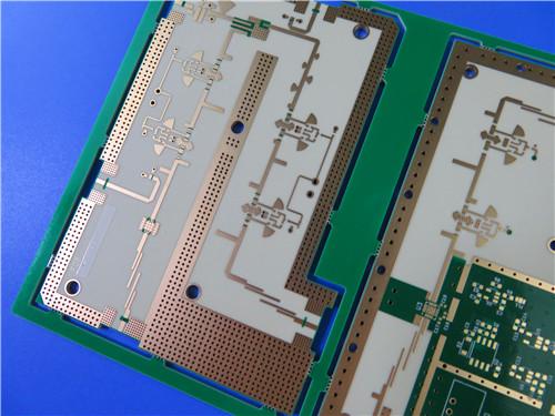
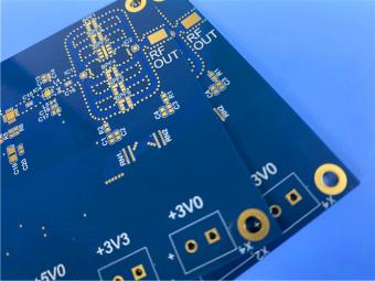
This 4-layer hybrid printed circuit board places an 8 mil (0.203 mm) Rogers RO4003C high-frequency core directly beneath the top RF layer, while Tg170 FR-4 carries the lower signal and digital sections, with the two cores bonded by a single sheet of 2116 prepreg. The result is a 0.556 mm (about 21.9 mil) finished board that gives RF and microwave traces a controlled, low-loss dielectric without the cost of an all-Rogers multilayer stack.
The build is supplied as 100 mm × 50 mm, 1 PCS, with 1 oz finished copper on the outer layers, 0.5 oz copper on the inner layers, a green solder mask on both faces, a white silkscreen on the top face and no bottom legend, and an Immersion Gold (ENIG) surface finish. Every board undergoes 100% electrical test before shipment. The construction is aimed at products that combine RF front-end circuitry with control and power routing on one board — matching networks, antenna feeds, RF identification and sensor front ends, and compact microwave modules.
Table 1 consolidates the controlled construction parameters of this build — the material system, layer count, format, copper weights, surface finish, legend and the test basis used for production.
|
Item |
Specification |
|
Base material |
Hybrid lamination – Rogers RO4003C high-frequency core + Tg170 FR-4 core and prepreg (mixed dielectric) |
|
Layer count |
4 layers |
|
Board dimensions |
100 mm × 50 mm = 1 PCS |
|
Finished board thickness |
0.556 mm (pressed), about 21.9 mil |
|
Dielectric build |
8 mil (0.203 mm) RO4003C core + 2116 prepreg (RC 53%), 0.12 mm after pressing + 5 mil (0.127 mm) Tg170 FR-4 core |
|
Finished Cu weight |
1 oz (35 µm) finished on outer layers; 0.5 oz (18 µm) on inner layers |
|
Surface finish |
Immersion Gold (ENIG) |
|
Top silkscreen |
White |
|
Bottom silkscreen |
None |
|
Top solder mask |
Green |
|
Bottom solder mask |
Green |
|
Electrical test |
100% electrical test (open / short / continuity) prior to shipment |
Table 1. Construction details of the 4-layer RO4003C / Tg170 FR-4 hybrid PCB.
Table 2 maps the layer-by-layer build: the8 mil RO4003C core forms the L1–L2 RF section, the 5 mil FR-4 core forms the L3–L4 section, and one 2116 prepreg bonds the two inner copper layers — the seven thicknesses sum exactly to the 0.556 mm pressed thickness.
|
Layer |
Material |
Thickness (mm) |
|
L1 — outer copper |
Copper, 1 oz finished (35 µm) |
0.035 |
|
L1–L2 dielectric |
Core RO4003C, 8 mil (0.203 mm) |
0.203 |
|
L2 — inner copper |
Copper, 0.5 oz (18 µm) |
0.018 |
|
L2–L3 bonding |
Prepreg 2116 (RC 53%), ×1 sheet |
0.120 |
|
L3 — inner copper |
Copper, 0.5 oz (18 µm) |
0.018 |
|
L3–L4 dielectric |
Core FR-4, Tg170, 5 mil (0.127 mm) |
0.127 |
|
L4 — outer copper |
Copper, 1 oz finished (35 µm) |
0.035 |
|
Pressed thickness |
Total finished board thickness |
0.556 |
Table 2. As-built layer stackup: dielectric total 0.450 mm + copper total 0.106 mm = 0.556 mm.
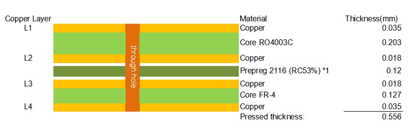
Figure 1. Engineering stackup drawing for the 4-layer hybrid build (L1 at top).
The defining choice is the dielectric under L1. RO4003C is a woven-glass-reinforced hydrocarbon/ceramic laminate (not PTFE) with a process dielectric constant of 3.38 ± 0.05 at 10 GHz, a design Dk of 3.55 across 8–40 GHz and a dissipation factor of just 0.0027 at 10 GHz — roughly 5.5 to 7 times lower than conventional FR-4 (Df about 0.015–0.020). Routing the RF path on L1 over the L2 reference plane therefore gives substantially lower insertion loss and tighter impedance control than the same geometry on an all-FR-4 board, while a thermal coefficient of Dk of only +40 ppm/°C from −50 to 150 °C keeps filters and matching networks centred over temperature.
The 8 mil (0.203 mm) gauge is also a deliberate impedance choice. On this core, a 50 Ω microstrip at 1 oz copper requires a trace width of only about 0.38 mm (15 mil), well within standard fabrication capability, and the core is a stocked standard gauge (0.008 in ± 0.0010 in), which keeps availability and lead time predictable.
An all-Rogers 4-layer stack is rarely necessary: the layers below L2 mostly carry power, control and digital signals that do not need a 3.38 Dk dielectric. This build therefore uses two 5-mil-class Tg170 FR-4 members — one sheet of 2116 prepreg (53% resin content, 0.12 mm after pressing) that bonds the inner copper layers, and one 5 mil (0.127 mm) FR-4 core that forms the L3–L4 pair. They add the dielectric thickness needed for the 0.556 mm target while placing premium material only where the RF field actually travels.
The Tg 170 °C FR-4 is qualified for lead-free assembly, so thehybrid circuitboard survives repeated lead-free reflow cycles without the resin softening, delamination or pad-cratering associated with lower-Tg grades. The result is a cost-optimised mixed-signal board with the same SMT process window as a standard FR-4 product.
Hybrid lamination is a process-controlled product, not simply a material choice. RO4003C expands at 11 and 14 ppm/°C in the X and Y axes — close to copper — with a 46 ppm/°C Z-axis value, while the Tg170 FR-4 members show a different expansion response, and the stack is mechanically asymmetric (0.203 mm ceramic core on one side, 0.127 mm FR-4 core on the other). Running a standard FR-4 press recipe through this material set could leave the mismatch visible as panel bow or twist, or as inner-layer delamination.
Production therefore uses a dedicated hybrid press profile — controlled ramp, dwell and cooling under defined pressure, with lay-up and resin-content control for the 2116 sheet — so the ceramic core and FR-4 move together through the glass transition. The result is a flat thin board with reliable plated through-holes, and the low Z-axis expansion of RO4003C supports barrel integrity under thermal shock.
The exposed outer copper is protected by ENIG (electroless nickel / immersion gold), which gives a flat, planar pad surface for fine-pitch SMT and BGA assembly, long shelf life and consistent solderability, and which is also suitable for contact and wire-bond surfaces.
· Cellular base-station antennas, feed networks and power amplifiers
· RF and microwave front-end modules combining RF with digital control
· RFID reader boards and antenna structures
· Automotive radar and sensor front ends
· LNBs for direct-broadcast satellite and other microwave receivers
This 4-layer RO4003C FR-4 hybrid PCB is a cost-engineered RF platform rather than a generic multilayer board: an 8 mil RO4003C core placed precisely under the RF layer, two 5-mil-class Tg170 FR-4 members carrying the remaining dielectric, a controlled hybrid press that manages the CTE mismatch, and a fixed-gauge build that delivers 0.556 mm repeatably.
With 1 oz finished outer and 0.5 oz inner copper, ENIG, green solder mask, a white top legend and 100% electrical test, the board combines microwave-grade low-loss performance on the signal-critical layer with FR-4 economics and lead-free assembly compatibility on the rest — a practical, manufacturable solution for volume RF and mixed-signal products.
The electrical performance of the board above is set by the laminate beneath it. This part documents Rogers RO4003C independently of the finished board so it can be used as a standalone material-selection reference.
RO4003C is part of the Rogers RO4000 series of high-frequency circuit materials. It is a proprietary woven-glass-reinforced hydrocarbon/ceramic laminate — it is not PTFE-based. The ceramic-filled, glass-reinforced resin system was engineered to deliver microwave-grade electrical performance while retaining the manufacturing behaviour of conventional epoxy/glass (FR-4), at a fraction of the cost of PTFE-based substrates. The laminate is offered in configurations using 1080 and 1674 glass fabric styles, all meeting the same electrical specification, and it conforms to IPC-4103 slash sheet /10.
As a rigid, thermoset laminate, RO4003C runs on standard FR-4 equipment: unlike PTFE materials, it requires no sodium-etch or specialised through-hole preparation, and it is compatible with automated handling and copper-surface scrubbing. It is CAF resistant and lead-free process compatible. The material is non-brominated and is not UL 94 V-0 rated; where a V-0 flame rating is mandatory, the flame-retardant sister grade RO4350B (or RO4835) is the specified alternative.
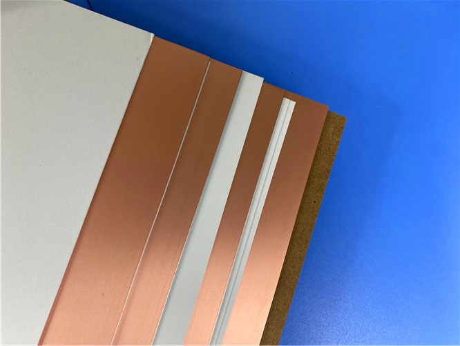
Figure 2. RO4000-series high-frequency copper clad laminate panels — bare copper-clad stock before circuit fabrication.
Table 3 presents the complete published typical property set for RO4003C — electrical, thermal, mechanical and physical — with direction, test conditions and test method. Values are typical of the production population; for specification limits, designers should consult Rogers Corporation.
|
Property |
Typical value |
Dir. |
Units |
Condition / test method |
|
Dielectric constant, εr (process) |
3.38 ± 0.05 |
Z |
— |
10 GHz / 23 °C; IPC-TM-650 2.5.5.5 clamped stripline |
|
Dielectric constant, εr (design) |
3.55 |
Z |
— |
8–40 GHz; differential phase length method |
|
Dissipation factor, tan δ |
0.0027 / 0.0021 |
Z |
— |
10 GHz / 2.5 GHz, 23 °C; IPC-TM-650 2.5.5.5 |
|
Thermal coefficient of εr |
+40 |
Z |
ppm/°C |
−50 to 150 °C; IPC-TM-650 2.5.5.5 |
|
Volume resistivity |
1.7 × 10¹⁰ |
— |
MΩ·cm |
Condition A; IPC-TM-650 2.5.17.1 |
|
Surface resistivity |
4.2 × 10⁹ |
— |
MΩ |
Condition A; IPC-TM-650 2.5.17.1 |
|
Electrical strength |
31.2 (780) |
Z |
kV/mm (V/mil) |
0.51 mm (0.020 in) sample; IPC-TM-650 2.5.6.2 |
|
Tensile modulus |
19,650 / 19,450 (2,850 / 2,821) |
X / Y |
MPa (ksi) |
RT; ASTM D638 |
|
Tensile strength |
139 / 100 (20.2 / 14.5) |
X / Y |
MPa (ksi) |
RT; ASTM D638 |
|
Flexural strength |
276 (40) |
— |
MPa (kpsi) |
IPC-TM-650 2.4.4 |
|
Dimensional stability |
< 0.3 |
X, Y |
mm/m (mils/in) |
After etch + E2/150 °C; IPC-TM-650 2.4.39A |
|
Coefficient of thermal expansion |
11 / 14 / 46 |
X / Y / Z |
ppm/°C |
−55 to 288 °C; IPC-TM-650 2.4.41 |
|
Tg (glass transition) |
> 280 |
— |
°C (TMA) |
IPC-TM-650 2.4.24.3 |
|
Td (decomposition) |
425 |
— |
°C (TGA) |
ASTM D3850 |
|
Thermal conductivity |
0.71 |
— |
W/(m·K) |
80 °C; ASTM C518 |
|
Moisture absorption |
0.06 |
— |
% |
48 h immersion, 0.060 in sample, 50 °C; ASTM D570 |
|
Density |
1.79 |
— |
g/cm³ |
23 °C; ASTM D792 |
|
Copper peel strength |
1.05 (6.0) |
— |
N/mm (pli) |
After solder float, 1 oz EDC foil; IPC-TM-650 2.4.8 |
|
Flammability |
Not rated (non-brominated) |
— |
— |
UL 94 — not V-0; use RO4350B / RO4835 for V-0 |
|
Lead-free process compatible |
Yes |
— |
— |
— |
Table 3. RO4003C typical properties (Rogers RO4000 series data sheet, PUB 92-004).
Table 4 lists the standard RO4003C gauges, panel formats and claddings; the 8 mil (0.203 mm) core used in the featuredhybrid PCB is a standard, stocked configuration.
|
Category |
Standard offering |
|
Dielectric thicknesses |
0.008 in (0.203 mm) ±0.0010 ← this build |
|
Standard panel sizes |
24 × 18 in (610 × 457 mm) |
|
Copper claddings |
Electrodeposited copper foil: ½ oz (18 µm) HH/HH; 1 oz (35 µm) H1/H1 |
Table 4. Standard RO4003C configurations (Rogers data sheet).
The three charts below illustrate the properties that drive RO4003C selection in RF and microwave work: a dielectric constant that stays nearly constant with temperature, a Dk that is flat over frequency, and low microstrip insertion loss.
Dielectric stability over temperature. Figure 3 shows RO4003C remaining essentially flat at about 3.38 across −50 to 150 °C, where PTFE/woven glass shows a pronounced step and slope near room temperature. Quantified by the +40 ppm/°C thermal coefficient, a 200 °C swing shifts Dk by less than 0.9% — essential for oscillators, filters and antennas whose resonant frequency must not drift with the environment.
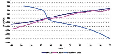
Figure 3. Dielectric constant vs. temperature — RO4003C vs. RO4350B and PTFE/woven glass (Rogers).
Dielectric stability over frequency. Figure 4 presents microstrip differential-phase-length measurements: the Dk extracted for 20 mil RO4003C stays flat from below 1 GHz to beyond 40 GHz, which is why the design Dk of 3.55 can be used across 8–40 GHz rather than being re-derived for each band. The flat response lets one material specification serve multi-band front ends covering sub-6 GHz and microwave bands alike.
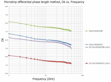
Figure 4. Dielectric constant vs. frequency, microstrip differential phase length method (Rogers).
Low insertion loss. Figure 5 plots microstrip insertion loss for the RO4000 family; the low-loss curves, together with the 0.0027 dissipation factor at 10 GHz, translate directly into lower attenuation per trace length, lower power-amplifier demand and lower thermal loading. For the lowest-loss option, LoPro reverse-treated foil is available and shifts the loss curve further downward.
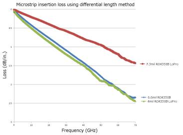
Figure 5. Microstrip insertion loss vs. frequency, differential length method (Rogers).
RO4003C substrate 's in-plane CTE of 11 and 14 ppm/°C (X/Y) is close to copper, which underwrites the reported dimensional stability of <0.3 mm/m after etching and thermal conditioning and gives the laminate excellent registration through multilayer processing. The 46 ppm/°C Z-axis value is low enough to support reliable plated through-holes even in severe thermal shock, and a Tg above 280 °C means expansion behaviour stays stable across the entire circuit-processing temperature range. Decomposition begins at 425 °C (TGA), and thermal conductivity of 0.71 W/(m·K) helps conduct heat away from dissipative components.
Mechanical integrity is reflected in a flexural strength of 276 MPa and a copper peel strength of 1.05 N/mm (6 pli) after solder float, which retains fine traces and pads. Moisture absorption of only 0.06% after 48 hours at 50 °C keeps electrical behaviour stable in humid service, and the laminate is documented as CAF resistant, supporting high-density via arrangements.
RO4003C is processed on standard epoxy/glass (FR-4) lines with no sodium-etch or specialised via preparation; it is lead-free process compatible, and LoPro reverse-treated foil (for reduced insertion loss) adds approximately 0.0007 in (18 µm) per core using a modified resin with a resin Dk of about 2.4. The material conforms to IPC-4103 slash sheet /10. Designers should note that RO4003C is non-brominated and not UL 94 V-0 rated; RO4350B or RO4835 should be specified where a V-0 flame rating is mandatory.
For space and aerospace use, Rogers laminates are evaluated under NASA test procedure SP-R-0022A (copper-etched specimens held 24 hours at 125 °C under vacuum of 10⁻⁶ torr or better). Materials with Total Mass Loss below 1.0% and Collected Volatile Condensable Materials below 0.1% are classified as low outgassing; RO4003C comfortably meets both limits, as shown in Table 5.
|
Material |
TML % |
CVCM % |
WVR % |
|
RO4003C |
0.06 |
0.00 |
0.02 |
|
RO4350B (reference) |
0.12 |
0.02 |
0.02 |
|
NASA SP-R-0022A limit |
< 1.0 |
< 0.1 |
Reporting optional |
Table 5. NASA SP-R-0022A outgassing results at 125 °C, ≤10⁻⁶ torr.
The same property set that makes RO4003C a good RF laminate also makes it a good hybrid partner. Its in-plane CTE sits near copper and near the values that FR-4 fabrications are designed to accommodate, while its dimensional stability (<0.3 mm/m after etch and bake) means inner-layer features remain predictable after lamination. Because it is a rigid, thermoset, FR-4-processable laminate rather than a soft PTFE sheet, it can be drilled, plated, laminated and routed on conventional equipment with standard bonding prepregs — the physical basis on which mixed-dielectric stacks such as an RO4003C core bonded to FR-4 cores can be manufactured at volume without exotic processes.
The practical result is a design rule: put RO4003C under the layers that carry RF fields and controlled-impedance lines, where its Dk 3.38 ± 0.05 and Df 0.0027 directly set electrical performance, and use FR-4 for the layers that only need mechanical support and ordinary signal routing. The laminates share a common process window, and the hybrid presses the two materials into one panel with controlled yield.
RO4003C occupies a deliberate position in the high-frequency laminate market: PTFE-class dielectric constant and loss, a Dk that is stable with both temperature and frequency, copper-matched thermal expansion, documented low outgassing and high Tg, combined with the processing economics and equipment of FR-4. Its full property set is published across electrical, thermal, mechanical and physical domains (Table 3), and the 8 mil (0.203 mm) gauge used in the featured board is a stocked standard thickness with standard ½ oz and 1 oz copper cladding.
These characteristics are precisely what make an8 mil RO4003C + Tg170 FR-4 hybridPCB stack viable: RO4003C supplies the controlled microwave environment for the RF layer, while FR-4 supplies the remaining dielectric at lower cost. For non-flame-rated RF, antenna, sensor and microwave-module designs, RO4003C is a well-supported, manufacturing-friendly and cost-effective high-frequency laminate.

Previous:
6-Layer 5mil Rogers RO3003 Mixed-Laminated with Isola 370HR 0.82 mm Hybrid PCB with ENIGNext:
8-Layer Hybrid RF PCB: RO4350B + TG170 FR-4 + RO4003C with RO4450F BondplyIf you have questions or suggestions,please leave us a message,we will reply you as soon as we can!
Categories
New Products
6-Layer 5mil Rogers RO3003 Mixed-Laminated with Isola 370HR 0.82 mm Hybrid PCB with ENIG
4-Layer 8mil RO4003C + Tg170 FR-4 Hybrid PCB with ENIG — 0.556mm Thin Build
1100 × 350mm Long-Format Rogers RO4003C 32 mil core Double-Sided High-Frequency PCB
Wangling TP2200 PCB 0.8mm Substrate Immersion Gold 2-Layer High-Dk (Dk 22) RF Board
Rogers TMM10 PCB 5.08mm Core ENIG 2-Layer High-Dk Microwave Board
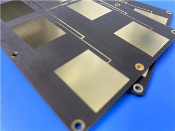
Taconic TLX-8 PCB 50mil ENIG 2-Layer High-Frequency RF Circuit Board
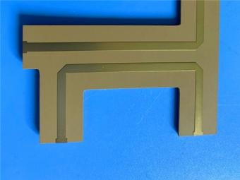
Wangling TF440 25mil DK4.4 Laminate Immersion Gold 2-Layer Copper-filling Vias PCB
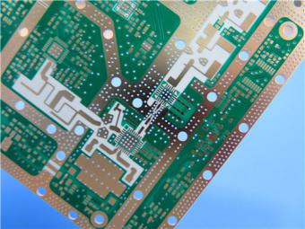
RO4360G2 Rogers 12mil ENEPIG 2-Layer DK6.15 High Frequency Custom PCB
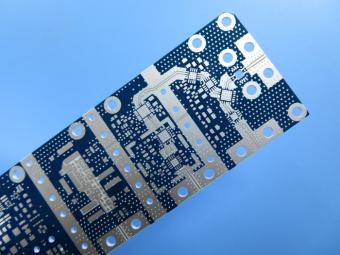
RO4003C exhibit a stable dielectric constant over a broad frequency range. This makes it an ideal substrate for broadband applications. And signal integrity performance improvement over the stack-ups with all FR4 board.
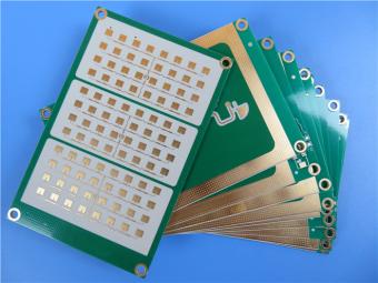
The hybrid PCB can be a mixture of FR-4 and high frequency material, and a mixture of high frequency material with different dielectric constant (DK)
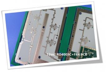
The 12mil core is on the top layer and it mainly plays the roles of signal layer. The core has fixed thickness which is very important to the electrical length of RF lines on the circuit board.
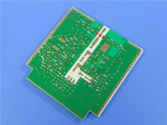
The hybrid PCB can be a mixture of FR-4 and high frequency material as abovementioned.
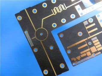
It contains 2 different boards in the panel. PCB boards are manufactured strictly as per required specifications with the standard IPC-Class-II.
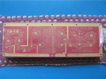
Hybrid PCB is also known as mixed material lamination, it’s normally combined by two different material like FR4 and PI(rigid flex PCB), FR4 and Ceramic, FR4 and Teflon, FR4 and Aluminum base etc.
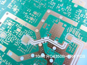
Hybrid constructions PCB typically involve a low loss material such as Nelco or Rogers combined with another core material like FR-4.
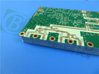
The Hybrid PCB on RO3003 and High Tg FR-4 is a state-of-the-art solution for high-frequency applications. With its exceptional stability, reliability, and manufacturability, it caters to the demands of industries such as automotive, telecommunications, and satellite communications.
 6-11C Shidai Jingyuan, Fuyong, Baoan, Shenzhen, Guangdong, China 518103


For inquiries about our products or pricelist, please leave to us and we will be in touch within 24 hours.
© Copyright: 2026 Shenzhen Bicheng Electronics Technology Co., Ltd.. All Rights Reserved.

IPv6 network supported


