

 Call Us Now !
Tel : +86 755 27374946
Call Us Now !
Tel : +86 755 27374946
 Order Online Now !
Email : info@bichengpcb.com
Order Online Now !
Email : info@bichengpcb.com
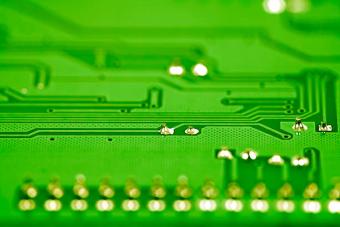
Whether you're developing satellite communication equipment or high-frequency radar systems,the F4BM217 high frequency PCB delivers the performance, reliability, and cost-efficiency you need.
Item NO.:
BIC-473-v559.0Order(MOQ):
1-10Payment:
T/TProduct Origin:
ChinaShipping Port:
ShenzhenLead Time:
7-10 days
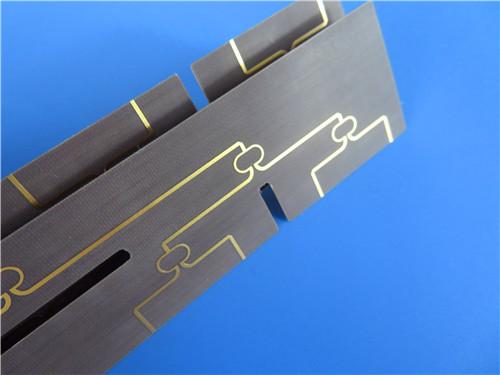
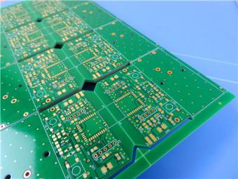
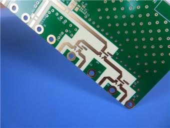
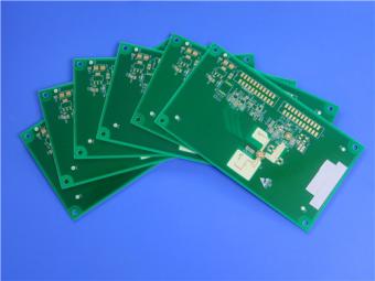
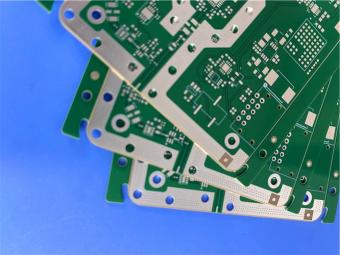
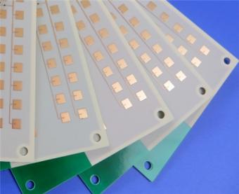
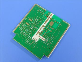
Wangling 2-layer F4BM217 3.9mil F4B DK2.17 High Frequency Laminate ENIG PCB
Designed for demanding high-frequency and RF applications, our 2-Layer F4BM217 PCB with 3.9mil ENIG surface finish stands out with exceptional electrical performance, precise manufacturing, and reliable quality. Leveraging Wangling F4BM217 laminates, this double-sided F4B DK2.17 PCB delivers low dielectric loss, stable insulation performance, and excellent dimensional stability, making it a cost-effective alternative to premium foreign counterparts. Compliant with IPC-Class-2 standards and available worldwide, it is engineered to meet the rigorous requirements of microwave, radar, and satellite communication systems.
PCB Construction Details
Below is a comprehensive overview of the F4BM217 PCB's construction parameters, manufacturing tolerances, and quality assurance measures, ensuring transparency and reliability for our customers.
|
Parameter |
Specification |
|
Base Material |
F4BM217 High-Frequency Laminate |
|
Layer Count |
2 (Double-Sided) |
|
Board Dimensions |
120mm x 89mm (±0.15mm) |
|
Finished Board Thickness |
0.17mm (Nominal) |
|
Minimum Trace Width / Spacing |
6 mils / 7 mils |
|
Minimum Mechanical Hole Size |
0.3mm |
|
Via Structure |
Through-Hole Vias Only (No Blind/Buried) |
|
Finished Copper Weight (Outer Layers) |
1 oz (35 μm / 1.4 mils) |
|
Via Plating Thickness |
20 μm (Minimum) |
|
Surface Finish |
Immersion Gold (ENIG) |
|
Top / Bottom Solder Mask |
No |
|
Top / Bottom Silkscreen |
No |
|
Electrical Test |
100% Testing (Pre-Shipment) |
PCB Stackup
The F4BM217 ENIG PCB adopts a simplified yet robust 2-layer rigid structure, with precisely controlled layer thicknesses to optimize electrical performance and mechanical reliability.
|
Layer |
Material |
Thickness |
|
Top Layer |
Copper (Electrodeposited) |
35 μm (1 oz) |
|
Dielectric Core |
F4BM217 Laminate |
0.10 mm |
|
Bottom Layer |
Copper (Electrodeposited) |
35 μm (1 oz) |
|
Total Finished Thickness |
|
~0.17 mm |
PCB Statistics
The following statistics reflect the PCB's streamlined design, tailored for focused functionality in high-frequency passive and active component integration.
|
Item |
Quantity |
|
Total Components |
5 |
|
Total Pads |
21 |
|
Through-Hole Pads |
15 |
|
Surface-Mount (SMT) Pads - Top Side |
6 |
|
Surface-Mount (SMT) Pads - Bottom Side |
0 |
|
Total Vias |
25 |
|
Total Nets |
2 |

Advanced F4BM217 Substrate: The Core of Superior Performance
The PCB is built on Wangling's F4BM217 substrates, a scientifically formulated composite of fiberglass cloth, polytetrafluoroethylene (PTFE) resin, and PTFE film, manufactured through strict pressing processes. Compared to F4B220, F4BM217 offers enhanced electrical performance with lower dielectric loss, higher insulation resistance, and improved stability. A key advantage lies in its flexible copper foil pairing: F4BM217 uses ED copper foil, ideal for applications without PIM requirements, while its variant F4BME217 (same dielectric layer) adopts reverse-treated foil (RTF) for excellent PIM performance and precise line control.
F4BM217 dielectric constant (Dk) is precisely controlled at 2.17±0.04 (10GHz) by adjusting the PTFE-fiberglass ratio, ensuring low signal loss. It features a dissipation factor of 0.001 (10GHz), minimal moisture absorption (≤0.08%), and UL-94 V0 flammability rating. With a wide operating temperature range of -55°C to 288°C and stable CTE values (25 ppm/°C x-axis, 34 ppm/°C y-axis), it maintains performance integrity in harsh environments.
Key Specifications & Global Availability
We provide Gerber RS-274-X artwork for seamless manufacturing integration. Adhering to IPC-Class-2 quality standards, every PCB undergoes rigorous inspection to ensure consistency. With worldwide availability, we offer timely delivery and localized support to customers across industries.
Typical Applications
This high-performance DK2.17 PCB is ideally suited for: Microwave, RF, and radar systems; Phase shifters; Passive components; Power dividers, couplers, and combiners; Feed networks; Phased array antennas; Satellite communications; Base station antennas.
Whether you're developing satellite communication equipment or high-frequency radar systems,the F4BM217 high frequency PCB delivers the performance, reliability, and cost-efficiency you need. Partner with us for a tailored solution that meets your most demanding application requirements.


Previous:
10mil Rogers RT/duroid 5880LZ 2-layer Immersion Gold White Silkscreen Custom BoardNext:
Wangling WL-CT350 PCB 2-layer 40mil 1.016mm ENIG Bare Copper High Frequency LaminatesIf you have questions or suggestions,please leave us a message,we will reply you as soon as we can!
Categories
New Products
12-layer TG200 TU-872 SLK High-Speed FR4 1.68mm PCB with ENIG Impedance Control
12-Layer RO4350B + RO3010 3.14mm Hybrid PCB Nickel-Free EPIG Surface Finish Blind Via
8-Layer Hybrid PCB RO4003C + S1000-2M FR4 with ENIG Surface Finish Blind Via
6-Layer Isola Astra MT77 PCB with Blind Via & Resin Plug Immersion Silver Finish
2-Layer 20mil FSD1020T ENIG High-Frequency PCB with Via Resin Plugged and Capped
4-Layer F4BM265+S1000-2M Material Hyrbid PCB with Blind Via Impedance Control & ENIG
4-Layer Wangling WL-CT338 + FR4 Hybrid PCB ENIG Green Solder Mask White Silkscreen
6-layer Isola 370HR High-Tg FR-4 PCB 2μ" ENIG Impedance Controlled

RF-10 25mil Taconic PCB Materials stands out as a high-performance solution for RF applications. Its exceptional electrical properties, dimensional stability, thermal conductivity, and adhesion characteristics make it an ideal choice for demanding applications.
The PCB has a 4-layer hybrid stackup with a 0.5oz+plating ground layer, two 1oz ground layers, and a 0.5oz+plating signal layer.
The dimensions of the board are 55.00 x 26.00 mm, with a tolerance of +/- 0.15mm. The board has 16 components, 26 total pads, 9 through-hole pads, 10 top SMT pads, 7 bottom SMT pads, 77 vias, and 82 nets.
Rogers RO4003C PCB is an innovative and advanced circuit board that is made with high-quality materials.
The RO4350B PCB offers a range of benefits that make it an ideal choice for high-frequency applications. Its low dielectric loss and high thermal conductivity make it perfect for high-frequency applications such as RF and microwave circuits.
Bicheng PCB Ships High-Quality PCBs with Shengyi Tg150 ℃ S1000H Material and Advanced Stackup
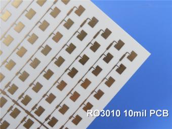
Rogers RO3010 PCB is ideal for a wide range of high-frequency applications, including power amplifiers, filters, couplers, and antennas.
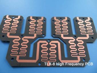
TLX-8 features low dielectric loss, low moisture absorption, and excellent thermal stability, making it ideal for high-frequency and high-speed applications. It has a low dissipation factor, which helps to minimize signal loss and distortion.
 6-11C Shidai Jingyuan, Fuyong, Baoan, Shenzhen, Guangdong, China 518103


For inquiries about our products or pricelist, please leave to us and we will be in touch within 24 hours.
© Copyright: 2026 Shenzhen Bicheng Electronics Technology Co., Ltd.. All Rights Reserved.

IPv6 network supported


