

 Call Us Now !
Tel : +86 755 27374946
Call Us Now !
Tel : +86 755 27374946
 Order Online Now !
Email : info@bichengpcb.com
Order Online Now !
Email : info@bichengpcb.com
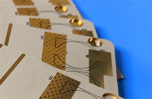
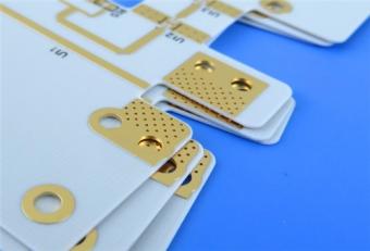
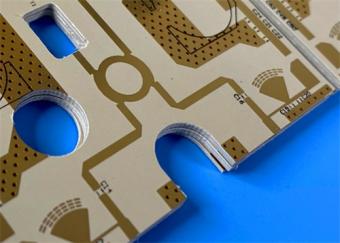
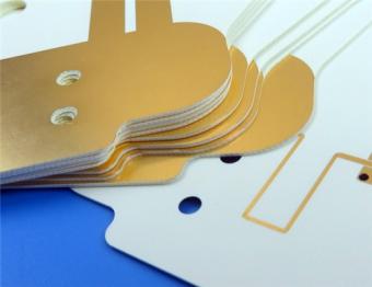
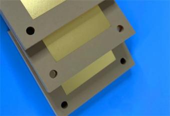
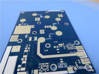
This custom-manufactured 2-layer rigid high-frequency PCB adopts Wangling WL-CT300 hydrocarbon ceramic copper clad laminate (CCL) with a ultra-thin 0.127mm (5mil) dielectric core and pure electroplated gold surface finish, engineered for high-stability RF, microwave, satellite and automotive radar circuit designs.
Item NO.:
BIC-574-v659.0Order(MOQ):
1-10Payment:
T/TProduct Origin:
ChinaShipping Port:
ShenzhenLead Time:
7-10 days
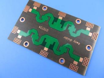
Wangling WL-CT300 5mil Laminate Pure Gold Plating High Frequency PCB
1. Product Overview
This custom-manufactured 2-layer rigid high-frequency PCB adopts Wangling WL-CT300 hydrocarbon ceramic copper clad laminate (CCL) with a ultra-thin 0.127mm (5mil) dielectric core and pure electroplated gold surface finish, engineered for high-stability RF, microwave, satellite and automotive radar circuit designs. Distinguished from conventional FR4 and expensive PTFE high-frequency boards, this 5mil Wangling PCB balances superior low-loss radio frequency performance, FR4-compatible manufacturability, tight dimensional tolerance, and long-term environmental reliability.
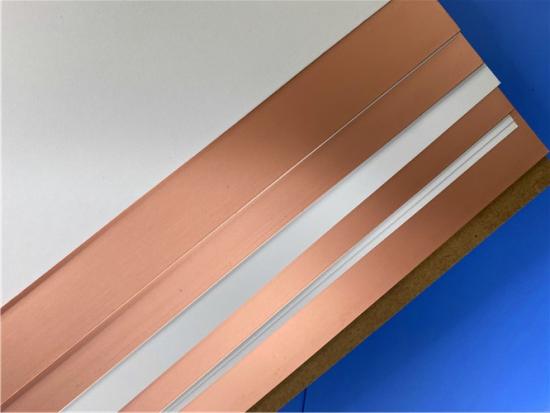
Unlike standard immersion gold or electroless nickel gold (ENIG) RF PCBs, this unit uses full pure gold plating for all exposed copper pads and vias, delivering ultra-low contact resistance, zero oxidation risk, and consistent impedance stability across 0.5–25GHz operating bands.
The ultra-thin 0.25mm finished board thickness caters to miniaturized RF module packaging demands, while matched copper-CCL thermal expansion coefficients eliminate thermal delamination and microvia cracking under wide temperature cycling (-55℃to 260℃long-term working range).
This article systematically elaborates the PCB structural specifications, stackup architecture, circuit statistics, core manufacturing differentiators, applicable industry scenarios, followed by a dedicated, detailed technical breakdown of the base WL-CT300 CCL with complete datasheet tables and performance curve illustrations, separating PCB finished board and raw substrate content without data repetition.
2. PCB Construction Details
This table summarizes all mechanical, electrical and surface finish manufacturing parameters of the finished WL-CT300 PCB, covering dimensional tolerance, trace geometry, thickness control, plating specifications and quality inspection protocols.
|
Parameter |
Specification |
|
Base Material |
WL-CT300 |
|
Board Dimensions |
66.04mm × 43.18mm (1 piece), ±0.15mm |
|
Minimum Trace/Space |
4/5 mils |
|
Minimum Hole Size |
0.25mm |
|
Blind Vias |
None |
|
Finished Board Thickness |
0.25mm (approx. 10mil) |
|
Finished Copper Weight |
1oz (1.4 mils) outer layers |
|
Via Plating Thickness |
20μm |
|
Surface Finish |
Pure Gold Plating |
|
Top Silkscreen |
Black |
|
Bottom Silkscreen |
None |
|
Top Solder Mask |
None |
|
Bottom Solder Mask |
None |
|
Electrical Testing |
100% prior to shipment |
3. PCB Stackup
This table clarifies the symmetrical 2-layer rigid stackup composition of the 5mil WL-CT300 PCB, listing copper foil thickness and core dielectric thickness layer by layer for impedance calculation and thermal stress analysis.
|
Layer |
Material/Description |
Thickness |
|
Copper Layer 1 |
Outer Layer Copper |
35 μm (1oz) |
|
Dielectric |
WL-CT300 Laminate |
0.127 mm (5mil) |
|
Copper Layer 2 |
Outer Layer Copper |
35 μm (1oz) |
4. PCB Statistical
This table quantifies all circuit feature counts of the finished PCB, including component mounting pads, vias, through-hole structures and signal nets to reflect its compact high-density RF circuit layout characteristics.
|
Metric |
Count |
|
Components |
36 |
|
Total Pads |
95 |
|
Through-Hole Pads |
56 |
|
Top SMT Pads |
39 |
|
Bottom SMT Pads |
0 |
|
Vias |
28 |
|
Nets |
2 |

5. Core Differentiated Product Advantages of 5mil WL-CT300 Pure Gold Plating PCB
5.1 Ultra-Low RF Loss Substrate Base Material
The core competitive edge of this PCB lies in the WL-CT300 thermosetting hydrocarbon ceramic composite core, which delivers Dk=3.00, Df=0.0025 at 10GHz. Compared with PTFE high-frequency boards, WL-CT300 supports full FR4-compatible PCB fabrication processes (drilling, etching, pressing, plating), cutting manufacturing cycle time and yield loss rate by over 30% while maintaining superior dielectric stability. Its TCDK value of 27ppm/℃ensures Dk variation below 0.008 within -55℃to 150℃, preventing impedance drift in outdoor radar and satellite communication equipment under extreme temperature shifts.
5.2 Pure Gold Plating Surface Finish for High-Reliability RF Circuits
Unlike conventional thin immersion gold (0.05–0.1μm Au), full pure gold plating forms a dense, inert conductive surface on all pads and vias with uniform thickness control. Gold’s natural anti-oxidation property eliminates copper oxide formation, which is a major source of passive intermodulation (PIM) distortion in antenna RF circuits. The finish retains ultra-low contact resistance under long-term humidity and vacuum environments, matching aerospace vacuum outgassing standards. Removing solder mask on both sides further eradicates dielectric loss introduced by liquid photoimageable solder mask (LPI), maximizing signal transmission efficiency at microwave frequency bands.
5.3 Ultra-Thin Rigid Structure with Optimized Thermal Stability
The finished 0.25mm total thickness is realized via the 5mil minimumWL-CT300 dielectric coreplus two layers of 1oz copper foil. X-axis CTE=15ppm/℃and Y-axis CTE=14ppm/℃perfectly match the thermal expansion coefficient of 35μm copper foil, preventing pad lifting, via barrel cracking and trace delamination after multiple 288℃solder reflow cycles (3 times, 10s each thermal stress test without delamination). The substrate’s Z-direction thermal conductivity reaches 0.41W/MK, far exceeding standard FR4 (0.2–0.3W/MK), offering passive heat dissipation for on-board power amplifier chips without additional heat sinks.
6. Typical Industrial Application
This 5mil WL-CT300 pure gold PCB targets high-performance radio frequency and microwave electronic equipment requiring stable signal integrity and long service life:
1)Communication Infrastructure: 5G/6G base station antennas, WiMAX distributed antenna systems, satellite high-frequency receiving heads, RF filters and power amplifier modules;
2)Automotive Electronics: Millimeter-wave automotive radar, vehicle navigation sensors, autonomous driving signal processing units;
3)Aerospace & Satellite: Spaceborne communication transceivers, phase-controlled phased array antennas, airborne early warning radar, vacuum aerospace equipment meeting low outgassing standards;
4)Microwave RF Devices: Passive RF filters, beam forming networks, low-noise signal transmission circuits with strict PIM control requirements.
7. Conclusion of Finished PCB
This 2-layer 5mil WL-CT300 PCB with full pure gold plating integrates low-loss hydrocarbon ceramic high-frequency substrate, precision fine-line manufacturing, anti-corrosion pure gold surface treatment and thermally matched stackup design, solving core pain points of conventional RF PCBs including large dielectric temperature drift, high PIM distortion, poor thermal stability and complex PTFE processing workflows. With verifiable, standardized mechanical, electrical and circuit statistical parameters, full IPC-Class-2 compliance and worldwide supply capacity, it serves as a cost-effective domestic alternative to imported foreign high-frequency PCB solutions for commercial RF, automotive radar and aerospace low-to-medium power microwave equipment. The ultra-thin 0.25mm profile, solder-mask-free design and pure gold finish further enhance miniaturization and long-term operational reliability in harsh temperature and humidity environments, making it a standardized custom high-frequency PCB platform for mass production and prototype verification.
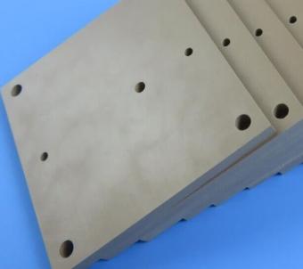
Appendix: Detailed Knowledge of the CCL Material (WL-CT300)
This section provides an in-depth technical overview of the copper-clad laminate (CCL) used as the core material for the PCB described above. While the PCB itself is fabricated on TF300, it is essential to understand the properties and capabilities of the broader material family, particularly the WL-CT300, which shares similar application spaces and offers a complementary set of advantages.
The following is a detailed technical datasheet for the WL-CT300 material, a hydrocarbon-ceramic-glass fabric composite designed for high-frequency applications.
1. Product Introduction
Wangling WL-CT series is a thermosetting resin system high-frequency material. The dielectric layer is composed of hydrocarbon resin, ceramics, and glass fabric. This composition provides low-loss performance suitable for high-frequency designs while offering PCB processability comparable to standard FR4 materials. Compared to PTFE-based materials,WL-CTPCB substrateseries is simpler to process, facilitating better circuit stability and consistency, and can serve as a direct replacement for similar international products.
The combination of hydrocarbon resin and composite ceramics provides excellent low-loss, high-temperature resistance, and temperature stability. This ensures that the material's dielectric constant and loss characteristics remain stable across a wide temperature range, with a low coefficient of thermal expansion (CTE) and a high glass transition temperature (Tg) exceeding 280°C.
The WL-CT series is available in dielectric constants of 3.00, 3.30, 3.38, 3.48, 4.10, and 6.15. It can be paired with ED copper foil or reverse-treated foil (RTF) copper foil. RTF copper foil offers excellent Passive Intermodulation (PIM) performance, reduces conductor loss, and minimizes insertion loss. It is applied with an adhesive backing that increases the material thickness by 0.018mm (0.7mil), ensuring good adhesion.
The series can also be combined with an aluminum substrate to form aluminum-based high-frequency materials. The PCB fabrication process can reference standard FR4 processing techniques. The material's excellent mechanical and physical properties allow for multiple lamination cycles, making it suitable for multilayer, high-layer-count, and backplane applications. It also demonstrates excellent processability for dense hole patterns and fine-line circuitry.
2. Product Features
1)Low Dielectric Constant Tolerance and Low Loss: Ensures consistent impedance control and minimal signal attenuation.
2)Hydrocarbon-Ceramic Thermosetting System: Provides superior PCB processability and heat resistance compared to thermoplastic alternatives.
3)Excellent Temperature Coefficient of Dielectric Constant (TCDK): The dielectric constant exhibits minimal variation with temperature changes.
4)Low Coefficient of Thermal Expansion (CTE): The CTE in the X and Y directions is matched to that of copper, while the Z-axis CTE is small, guaranteeing dimensional stability and plated through-hole reliability.
5)High Tg > 280°C: Maintains dimensional stability and plated through-hole quality even at elevated temperatures.
6)High Thermal Conductivity: Superior to comparable thermoplastic materials, making it suitable for high-power applications.
7)Commercial, High-Volume, Cost-Effective: Ideal for mass production.
8)Excellent Radiation Resistance: Maintains stable dielectric and physical properties after exposure to radiation.
9)Low Outgassing: Meets aerospace requirements for vacuum outgassing.

3. Typical Applications
4. WL-CT300 Complete Technical Datasheet
The following table provides a comprehensive list of the electrical, thermal, and mechanical properties of the WL-CT300 material.
|
Property |
Test Condition |
Unit |
WL-CT300 Value |
|
Dielectric Constant (Typical) |
10GHz |
— |
3 |
|
Dielectric Constant (Design) |
10GHz |
— |
2.98 |
|
Dielectric Constant Tolerance |
— |
— |
±0.05 |
|
Dissipation Factor |
2GHz |
— |
0.0025 |
|
10GHz |
— |
0.003 |
|
|
20GHz |
— |
0.0036 |
|
|
TCDK (Temperature Coefficient of Dk) |
-55°C to 150°C |
ppm/°C |
27 |
|
Peel Strength |
1oz ED Copper |
N/mm |
0.85 |
|
1oz RTF Copper |
N/mm |
0.72 |
|
|
Volume Resistivity |
Normal State |
MΩ·cm |
3×10⁸ |
|
Surface Resistance |
Normal State |
MΩ |
2×10⁸ |
|
Dielectric Strength (Z-direction) |
5kW, 500V/s |
kV/mm |
28 |
|
Breakdown Voltage (X-Y direction) |
5kW, 500V/s |
kV |
35 |
|
CTE (X-axis) |
-55°C to 288°C |
ppm/°C |
15 |
|
CTE (Y-axis) |
-55°C to 288°C |
ppm/°C |
14 |
|
CTE (Z-axis) |
-55°C to 288°C |
ppm/°C |
31 |
|
Thermal Stress |
288°C, 10s, 3 cycles |
— |
No Delamination |
|
Moisture Absorption |
20±2°C, 24 hours |
% |
0.15 |
|
Density |
Room Temperature |
g/cm³ |
1.57 |
|
Long-Term Operating Temperature |
— |
°C |
-55 to +260 |
|
Thermal Conductivity |
Z-direction |
W/(m·K) |
0.41 |
|
PIM (Passive Intermodulation) |
with RTF Copper |
dBc |
≤-158 |
|
Flammability |
UL-94 |
Rating |
V-0 |
|
TG (Glass Transition Temperature) |
— |
°C |
>280 |
|
TD (Thermal Decomposition) |
Onset |
°C |
412 |
|
Halogen Content |
— |
— |
Halogenated |
|
Material Composition |
— |
— |
Hydrocarbon + Ceramic + Fiberglass |
5. Available Constructions
Copper Foil Options
Thickness: 0.5 oz (0.018mm), 1 oz (0.035mm); other thicknesses available upon request.
Type: ED copper foil, RTF copper foil. (RTF foil includes an adhesive layer, increasing the substrate thickness by 0.018mm/0.7mil).
Available Panel Sizes
460×610mm (18×24″)
915×1220mm (36×48″)
WL-CT300 Dielectric Thickness and Tolerance
The base material is available in thicknesses starting from 0.127mm (5mil) and in multiples thereof. For thicknesses exceeding 3.05mm, please contact the factory for customization
|
Thickness (ED Copper) |
Tolerance |
Thickness (RTF Copper) |
Tolerance |
|
0.127mm (5.0mil) |
±0.012mm (0.5mil) |
0.272mm (10.7mil) |
±0.025mm (1.0mil) |
|
0.254mm (10mil) |
±0.025mm (1.0mil) |
0.526mm (20.7mil) |
±0.038mm (1.5mil) |
|
0.508mm (20mil) |
±0.038mm (1.5mil) |
0.780mm (30.7mil) |
±0.051mm (2.0mil) |
|
0.762mm (30mil) |
±0.050mm (2.0mil) |
1.034mm (40.7mil) |
±0.076mm (3.0mil) |
|
1.016mm (40mil) |
±0.076mm (3.0mil) |
1.542mm (60.7mil) |
±0.100mm (4.0mil) |
|
1.524mm (60mil) |
±0.100mm (4.0mil) |
2.050mm (80.7mil) |
±0.127mm (5.0mil) |
WL-CT Series Product Family
The Wangling WL-CT series offers a range of dielectric constants to suit diverse application requirements:
This product family enables designers to select the optimal dielectric constant for their specific impedance, size, and performance requirements while maintaining consistent processing characteristics across the series.
CONCLUSION
The WL-CT300 2-layer 5mil PCB with pure gold plating represents a thoughtfully engineered solution that bridges the gap between ultra-high-frequency performance and practical manufacturability. By combining Wangling's advanced hydrocarbon ceramic thermosetting laminate with precision fabrication parameters—4/5 mil trace/space, 0.25mm minimum hole size, 20μm via plating, and pure gold surface finish—this board delivers the electrical characteristics demanded by modern RF and microwave systems while remaining accessible through standard PCB fabrication channels.


If you have questions or suggestions,please leave us a message,we will reply you as soon as we can!
Categories
New Products
RO4835 20mil Rogers Laminate 2-layer Immersion Gold Custom PCB
Rogers 20mil DiClad 527 PCB 2-layer Immersion Gold No Solder Mask Black Silkscreen

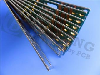
Wangling WL-CT300 5mil Laminate Pure Gold Plating High Frequency PCB
Wangling TF300 25mil DK3.0 Laminate 2-layer PCB Immersion Gold Black Silkscreen
2-Layer 0.5mm TP440 PCB Wangling TP DK4.4 Laminate Immersion Gold
20-Layer Panasonic TU872 HDI PCB ENEPIG 3.0mm Finished Thick Laser-drilled Blind Vias
10-Layer Rogers RO4003C + 370HR FR4 Hybrid Laminate PCB ENIG Impedance Control
8-Layer 10oz Heavy Copper TU-865 Substrate PCB With ENIG Blind &Buried Via
Polytetrafluoroethylene (Short for PTFE), commonly known as "plastic king ", is a polymer compound made of tetrafluoroethylene by polymerization. It has excellent chemical stability, corrosion resistance, sealing, high lubrication and non-viscosity, electrical insulation and good aging resistance.
Rogers TMM4 thermoset microwave material is ceramic, hydrocarbon, thermoset polymer composite designed for high plated-through-hole reliability stripline and microstrip applications.
Taconic TLY laminates are a type of low loss laminates. They are manufactured with very light weight woven fiberglass and are more dimensionally stable than chopped fiber reinforced PTFE composites.
RO3203 laminates combine the surface smoothness of a non-woven PTFE laminate, for finer line etching tolerances, with the rigidity of a woven-glass PTFE laminate. These materials can be fabricated into printed circuit boards using
This type of immersion silver RF PCB is made on one of Taconic’s ORCER family material: RF-45.
Rogers’ TMM10 thermoset microwave materials are ceramic, hydrocarbon, thermoset polymer composites designed for high plated-thru-hole reliability stripline and microstrip applications.
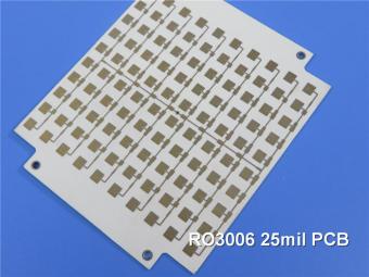
Rogers RO3006 was designed to offer exceptional electrical and mechanical stability at competitive prices.
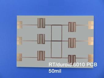
RT/duroid 6010LM microwave laminates feature ease of fabrication and stability in use. This property results in the possibility of mass production and reducing the cost of goods.
 6-11C Shidai Jingyuan, Fuyong, Baoan, Shenzhen, Guangdong, China 518103


For inquiries about our products or pricelist, please leave to us and we will be in touch within 24 hours.
© Copyright: 2026 Shenzhen Bicheng Electronics Technology Co., Ltd.. All Rights Reserved.

IPv6 network supported


