

 Call Us Now !
Tel : +86 755 27374946
Call Us Now !
Tel : +86 755 27374946
 Order Online Now !
Email : info@bichengpcb.com
Order Online Now !
Email : info@bichengpcb.com

The 2-layer 25mil TF300 high-frequency PCB is a highly targeted high-performance circuit product integrating excellent dielectric performance, reliable mechanical properties and convenient manufacturability.
Item NO.:
BIC-573-v658.0Order(MOQ):
1-10Payment:
T/TProduct Origin:
ChinaShipping Port:
ShenzhenLead Time:
7-10 days
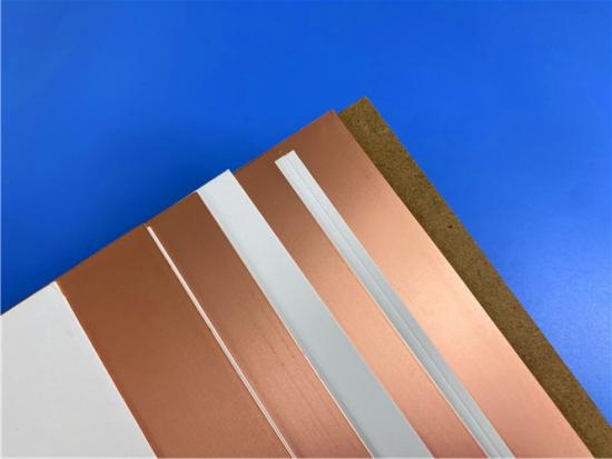
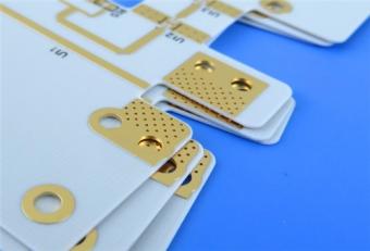
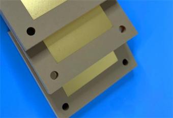
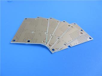
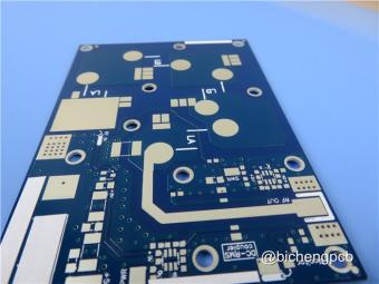
Wangling TF300 25mil DK3.0 Laminate 2-layer PCB Immersion Gold Black Silkscreen
Introduction
This is a 2-layer, 0.7mm thick rigid printed circuit board fabricated using Wangling TF300 high-frequency laminate. Designed for demanding microwave and millimeter-wave applications, this PCB leverages the unique properties of a PTFE-ceramic composite material to deliver exceptional electrical performance, thermal stability, and mechanical reliability. The following sections detail the TF300 board's construction, stackup, statistical data, and the underlying core material's properties, providing engineers and procurement specialists with the critical information needed for system integration and design validation.
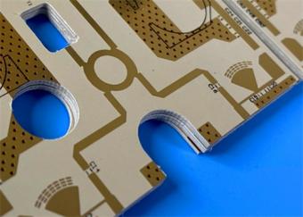
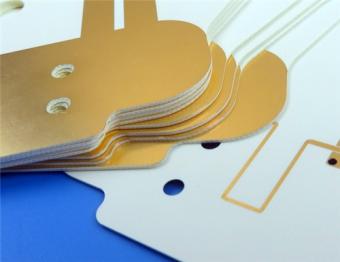
2. PCB Construction Details
The table below summarizes the key physical and manufacturing parameters of the Wangling PCB, defining its form factor, fabrication rules, and finish specifications.
|
Parameter Category |
Specific Specification |
|
Base Material |
TF300 |
|
Layer Count |
2 layers (rigid double-sided PCB) |
|
Board Dimension |
70mm × 49mm (1 piece), tolerance: ±0.15mm |
|
Minimum Trace/Space |
5/5 mils |
|
Minimum Hole Size |
0.3mm |
|
Via Type |
No blind vias (only through holes) |
|
Finished Board Thickness |
0.7mm |
|
Outer Layer Copper Weight |
1oz (1.4 mils / 35 μm) |
|
Via Plating Thickness |
20 μm |
|
Surface Finish |
Immersion Gold |
|
Silkscreen |
Top side: No; Bottom side: No |
|
Solder Mask |
Top side: No; Bottom side: No |
|
Pre-Shipment Inspection |
100% full electrical testing |
3. PCB Stackup
The stackup defines the layer structure and thickness of the materials used in the PCB construction.
|
Layer Sequence |
Material Type |
Thickness |
|
Copper Layer 1 (Top Outer Layer) |
Standard Electrolytic Copper Foil |
35 μm (1oz) |
|
Core Dielectric |
TF300 Substrate |
0.635 mm (25 mils) |
|
Copper Layer 2 (Bottom Outer Layer) |
Standard Electrolytic Copper Foil |
35 μm (1oz) |
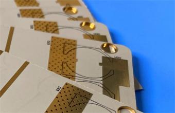
4. PCB Statistics
The following table provides a quantitative breakdown of the board's components and features.
|
Statistical Item |
Specific Quantity |
|
Total Mounted Components |
25 |
|
Total Pads |
66 |
|
Through-Hole Pads |
39 |
|
Top SMT Pads |
27 p |
|
Bottom SMT Pads |
0 |
|
Total Vias |
16 |
|
Total Nets |
2 |

5. Conclusion
In summary, the 2-layer 25mil TF300 high-frequency PCB is a highly targeted high-performance circuit product integrating excellent dielectric performance, reliable mechanical properties and convenient manufacturability. Its standardized construction parameters, symmetrical 2-layer stackup and reasonable circuit layout fully meet the design and use requirements of microwave, millimeter-wave, aerospace and radar equipment.
The adoption of fiberglass-free TF300 PTFE-ceramic CCL endows the board with core competitive advantages such as low loss, stable Dk, wide temperature resistance and anti-radiation, which cannot be matched by ordinary FR-4 and conventional glass fiber high-frequency PCBs.
Strict IPC-Class-2 quality control and 100% pre-delivery electrical testing ensure the long-term stability of products in harsh working environments. With reasonable structure, reliable performance and global supply capability, this Wangling DK3.0 PCB can effectively meet the procurement and application demands of high-end high-frequency electronic equipment manufacturers, and is a preferred high-frequency circuit carrier for mid-to-high-end wireless communication, aerospace and defense electronic fields.
Supplementary Knowledge: Detailed Introduction to TF300 PTFE-Ceramic Copper Clad Laminate (CCL)
1. Basic Overview of TF Series & TF300 CCL
TFlaminateseries is a high-frequency copper clad laminate independently developed by Wangling, a composite material made of polytetrafluoroethylene (PTFE) resin and ceramic fillers, with no fiberglass cloth added in the formula. By adjusting the mixing ratio of ceramic and PTFE resin, the dielectric constant of the material can be precisely calibrated. Combined with exclusive special production processes, the series delivers outstanding dielectric stability, ultra-low loss and high overall reliability. In the product classification, TF refers to non-copper-clad bare substrate, TF-1 refers to single-sided copper-clad laminate, and TF-2 refers to double-sided copper-clad laminate.
The TF300 model is the classic low-Dk product of the TF series, with a fixed dielectric constant of 3.0, focusing on high-frequency, low-loss and high-stability application scenarios, and is widely matched with high-frequency PCBs for microwave and aerospace use.
2. Core Features of TF Series CCL
1)Wide and stable dielectric constant range: The Dk of the entire TF series covers 3~16, with mainstream models including 3.0, 6.0, 9.2, 9.6, 10.2 and 16. All models feature high Dk stability and ultra-low dielectric loss, suitable for different high-frequency signal design requirements.
2)Excellent high-frequency adaptability: Specially developed for microwave and millimeter-wave printed circuits, it effectively reduces signal transmission loss and ensures signal integrity in high-frequency bands.
3)Ultra-wide temperature resistance: The long-term continuous operating temperature ranges from -80℃to +200℃, far exceeding the temperature resistance limit of ordinary epoxy substrates, adapting to extreme cold and high-temperature working environments.
4)Customizable thickness: Standard substrate thickness ranges from 0.635 mm to 2.5 mm, and non-standard thickness can be customized according to customer demands.
5)Special environmental resistance: It has excellent radiation resistance and low outgassing performance, complying with the strict material standards of space and aerospace equipment.
6)Good processability: It can be processed using standard thermoplastic material manufacturing methods, compatible with mainstream PCB production lines, without special process transformation, and has high production efficiency and yield.

3. Complete Technical Data Sheet of TF300 CCL
The following table lists all typical performance parameters, test conditions, units and standard values of TF300 CCL, with all data tested in accordance with GB/T 12636-1990, IPC-TM-650 and GBT4722-2017 standards.
|
Performance Item |
Test Condition |
Unit |
Standard Value of TF300 |
|
Dielectric Constant (Dk) |
10 GHz, Z-direction |
/ |
3.0±0.06 |
|
Dk Tolerance |
/ |
/ |
±2% |
|
Dissipation Factor (DF / Loss Tangent) |
10 GHz |
/ |
0.001 |
|
Thermal Coefficient of Dielectric Constant (TCDK) |
-55℃ ~ 150℃ |
ppm/℃ |
-60 |
|
Peel Strength (1 oz copper foil, normal state) |
Room temperature |
N/mm |
>0.6 |
|
Peel Strength (1 oz copper foil, after AC humidity test) |
After humidity aging test |
N/mm |
>0.4 |
|
Volume Resistivity |
Normal state, 500V |
MΩ·cm |
>1×10⁹ |
|
Surface Resistivity |
Normal state, 500V |
MΩ |
>1×10⁷ |
|
Coefficient of Thermal Expansion (CTE, X-axis) |
-55℃ ~ 150℃ |
ppm/℃ |
60 |
|
Coefficient of Thermal Expansion (CTE, Y-axis) |
-55℃ ~ 150℃ |
ppm/℃ |
60 |
|
Coefficient of Thermal Expansion (CTE, Z-axis) |
-55℃ ~ 150℃ |
ppm/℃ |
80 |
|
Water Absorption |
20±2℃, soaked for 24 hours |
% |
≤0.05 |
|
Long-Term Operating Temperature |
High-low temperature chamber |
℃ |
-80 ~ +200 |
|
Material Density |
Room temperature |
g/cm³ |
2.41 |
|
Thermal Conductivity |
Room temperature |
W/m·K |
0.3 |
|
Main Material Composition |
/ |
/ |
PTFE resin + ceramic filler + ED electrolytic copper foil |
4. Copper Foil & Size Specifications of TF300 CCL
4.1 Copper Foil Configuration
TF300 is matched with ED (electrolytic) copper foil, with two conventional copper foil thickness options:
0.018 mm (0.5 oz) and 0.035 mm (1 oz).
The 1 oz copper foil (0.035 mm) is the most commonly used model for high-frequency PCBs, which balances current-carrying capacity and fine-line production capability. The copper foil has strong adhesion with the dielectric substrate, and still maintains high peel strength after humidity and temperature cycling tests, avoiding copper foil warpage and detachment.
4.2 Standard Product Dimensions
The standard blank substrate sizes of TF300 CCL are 150 mm×150 mm and 250 mm×250 mm, which can meet the cutting demands of most small and medium-sized PCBs. For special-size boards, customized cutting services are supported.
4.3 Standard Thickness & Tolerance (Dielectric Core / Total Thickness Including Copper)
Customers need to clearly mark "dielectric core thickness" or "total thickness including copper" when placing orders. The standard thickness and tolerance are shown in the table below:
|
Standard Thickness (mm) |
0.635 |
0.8 |
1 |
1.2 |
1.5 |
2 |
2.5 |
|
Thickness Tolerance (mm) |
±0.04 |
±0.05 |
±0.05 |
±0.05 |
±0.06 |
±0.08 |
±0.01 |
5. Material Composition & Testing Standard Explanation
TF300 copper cld laminate is composed of high-purity PTFE resin and uniformly dispersed nano-ceramic fillers, with no fiberglass cloth added. This formula fundamentally eliminates the signal phase shift and loss increase caused by glass fiber texture in high-frequency transmission. The dielectric constant test adopts the stripline method specified by GB/T 12636-1990 or IPC-TM650 2.5.5.5, and all electrical, mechanical and environmental reliability tests refer to IPC-TM-650 or GBT4722-2017. All data in the specification are typical measured values, providing objective reference for customers to select materials. Customers need to verify the adaptability of TF300 CCL according to actual application scenarios.
6. Main Application Fields of TF300 CCL
As a low-Dk and low-loss high-frequency CCL, TF300 is mainly used to produce high-frequency PCBs for high-end fields:
Aerospace on-board equipment
Space equipment, aircraft cabin electronic equipment
Various microwave antennas and phase array antennas
Early warning radars and airborne radars
Beamforming networks
satellite communication and navigation systems, as well as RF power amplifiers.
Its multiple advantages such as radiation resistance, low outgassing, wide temperature resistance and stable high-frequency performance make it irreplaceable in high-reliability high-frequency electronic equipment.


Previous:
Wangling WL-CT300 5mil Laminate Pure Gold Plating High Frequency PCBNext:
2-Layer 0.5mm TP440 PCB Wangling TP DK4.4 Laminate Immersion GoldIf you have questions or suggestions,please leave us a message,we will reply you as soon as we can!
Categories
New Products
RO4835 20mil Rogers Laminate 2-layer Immersion Gold Custom PCB
Rogers 20mil DiClad 527 PCB 2-layer Immersion Gold No Solder Mask Black Silkscreen
Wangling WL-CT300 5mil Laminate Pure Gold Plating High Frequency PCB
Wangling TF300 25mil DK3.0 Laminate 2-layer PCB Immersion Gold Black Silkscreen
2-Layer 0.5mm TP440 PCB Wangling TP DK4.4 Laminate Immersion Gold
20-Layer Panasonic TU872 HDI PCB ENEPIG 3.0mm Finished Thick Laser-drilled Blind Vias
10-Layer Rogers RO4003C + 370HR FR4 Hybrid Laminate PCB ENIG Impedance Control
8-Layer 10oz Heavy Copper TU-865 Substrate PCB With ENIG Blind &Buried Via
Polytetrafluoroethylene (Short for PTFE), commonly known as "plastic king ", is a polymer compound made of tetrafluoroethylene by polymerization. It has excellent chemical stability, corrosion resistance, sealing, high lubrication and non-viscosity, electrical insulation and good aging resistance.
Rogers TMM4 thermoset microwave material is ceramic, hydrocarbon, thermoset polymer composite designed for high plated-through-hole reliability stripline and microstrip applications.
Taconic TLY laminates are a type of low loss laminates. They are manufactured with very light weight woven fiberglass and are more dimensionally stable than chopped fiber reinforced PTFE composites.
RO3203 laminates combine the surface smoothness of a non-woven PTFE laminate, for finer line etching tolerances, with the rigidity of a woven-glass PTFE laminate. These materials can be fabricated into printed circuit boards using
This type of immersion silver RF PCB is made on one of Taconic’s ORCER family material: RF-45.
Rogers’ TMM10 thermoset microwave materials are ceramic, hydrocarbon, thermoset polymer composites designed for high plated-thru-hole reliability stripline and microstrip applications.
Rogers RO3006 was designed to offer exceptional electrical and mechanical stability at competitive prices.
RT/duroid 6010LM microwave laminates feature ease of fabrication and stability in use. This property results in the possibility of mass production and reducing the cost of goods.
 6-11C Shidai Jingyuan, Fuyong, Baoan, Shenzhen, Guangdong, China 518103


For inquiries about our products or pricelist, please leave to us and we will be in touch within 24 hours.
© Copyright: 2026 Shenzhen Bicheng Electronics Technology Co., Ltd.. All Rights Reserved.

IPv6 network supported


