

 Call Us Now !
Tel : +86 755 27374946
Call Us Now !
Tel : +86 755 27374946
 Order Online Now !
Email : info@bichengpcb.com
Order Online Now !
Email : info@bichengpcb.com
TMM13i laminate represents a best-in-class balance of electrical performance, mechanical robustness, thermal stability, and manufacturing practicality.
Item NO.:
BIC-548-v633.0Order(MOQ):
1-10Payment:
T/TProduct Origin:
ChinaShipping Port:
ShenzhenLead Time:
7-10 days
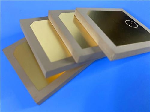
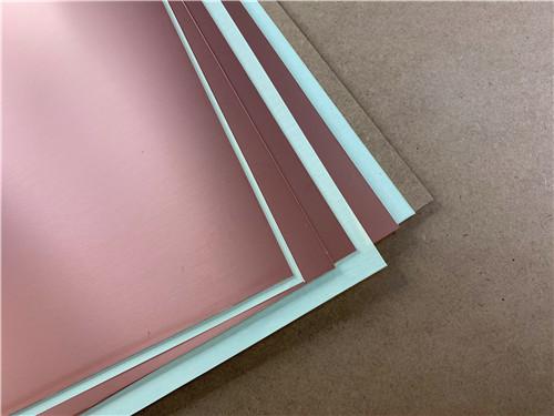
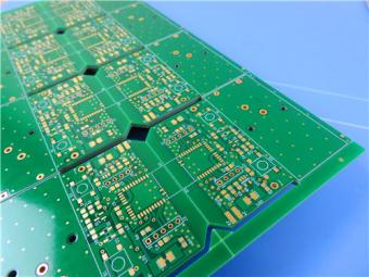
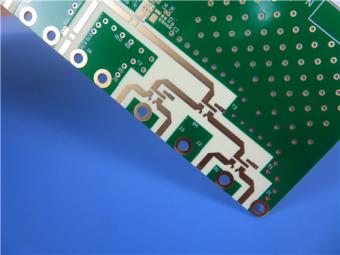
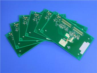
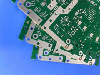
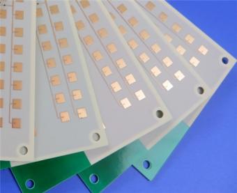
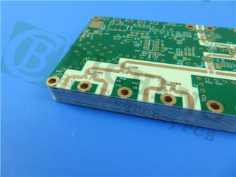
150mil Rogers TMM13i 2-layer ENIG Bare Copper Custom PCB
Introduction
This is ahigh-performance 2-layer rigid PCB built on Rogers 150mil TMM13i high-frequency ceramic-thermoset composite substrate, finished with ENIG (Electroless Nickel Immersion Gold) surface treatment and qualified to IPC-Class-2 standards. This 150 mil Rogers board is engineered for mission-critical RF, microwave, satellite communication, radar, and high-precision test applications requiring stable dielectric performance, matched thermal expansion, robust mechanical integrity, and long-term reliability under extreme thermal and chemical environments. Unlike standard FR-4 or low-performance microwave laminates, thisTMM13i PCB combines the electrical advantages of ceramic substrates with the manufacturability of conventional thermoset PCBs, eliminating the need for specialized PTFE-style processing while delivering exceptional high-frequency behavior.
1. PCB Construction Overview
This section summarizes the complete mechanical, electrical, and surface-finish configuration of the finished PCB, defining all critical fabrication parameters for performance and assembly compatibility.
|
Item |
Specification |
|
Base Material |
Rogers TMM13i |
|
Layer Count |
2 layers (rigid double-sided) |
|
Board Dimension |
76.8 mm × 97 mm (per piece) |
|
Minimum Trace / Space |
4 mils / 5 mils |
|
Minimum Hole Size |
0.25 mm |
|
Blind Vias |
Not used (No blind vias) |
|
Finished Board Thickness |
3.9 mm |
|
Finished Copper Weight (Outer Layers) |
1 oz (≈1.4 mils / 35 μm) |
|
Via Plating Thickness |
20 μm |
|
Surface Finish |
ENIG (Electroless Nickel Immersion Gold) |
|
Top Silkscreen |
No |
|
Bottom Silkscreen |
No |
|
Top Solder Mask |
No |
|
Bottom Solder Mask |
No |
|
Quality Assurance |
100% electrical test before shipment |
2. PCB Stack-Up Structure
The following table defines the symmetric layer structure that ensures consistent electrical performance, mechanical stability, and uniform thermal distribution across the board.
|
Layer |
Material |
Thickness |
|
Copper Layer 1 (Top) |
Electrodeposited copper |
35 μm (1 oz) |
|
Core Dielectric |
Rogers TMM13i |
3.81 mm (150mil) |
|
Copper Layer 2 (Bottom) |
Electrodeposited copper |
35 μm (1 oz) |
3. PCB Layout & Net Statistics
This table summarizes component, pad, via, and net density to support assembly planning, design verification, and manufacturing yield analysis.
|
Parameter |
Value |
|
Component Count |
29 |
|
Total Pads |
47 |
|
Through Hole Pads |
19 |
|
Top SMT Pads |
28 |
|
Bottom SMT Pads |
0 |
|
Vias |
26 |
|
Nets |
2 |

4. PCB Key Performance Advantages
4.1 High-Frequency Electrical Stability
TMM13i provides a tightly controlled isotropic dielectric constant Dk = 12.85±0.35 and dissipation factor Df = 0.0019 at 10 GHz, enabling predictable impedance control, low signal distortion, and high efficiency in microstrip and stripline circuits. Its low thermal coefficient of dielectric constant (TCDk =–70 ppm/°K) preserves electrical performance across wide operating temperatures, critical for radar, satellite, and automotive applications.
4.2 Thermal & Mechanical Reliability
The CTE of TMM13i is closely matched to copper: X-axis 19 ppm/°C, Y-axis 19 ppm/°C, Z-axis 20 ppm/°C over–55 to +288°C, minimizing thermal stress on plated through holes (PTHs) and vias during thermal cycling and reflow. The thermoset matrix prevents substrate softening at soldering temperatures, enabling reliable wire bonding without pad lifting or deformation. The material also exhibits high resistance to process chemicals, reducing damage during plating and etching.
4.3 ENIG Surface Finish Benefits
ENIG provides a flat, noble-metal surface ideal for fine-pitch SMT, QFN, BGA, and chip-on-board assembly. The nickel barrier layer (typically 3–6μm) blocks copper diffusion, while the thin immersion gold layer (0.05–0.15μm) preserves solderability during storage and multiple reflow cycles. ENIG supports Al wire bonding and offers excellent contact stability for RF signal pads and test points, making it superior to OSP, HASL, or immersion silver for high-reliability microwave assemblies.
Appendix: Rogers TMM13i CCL (Copper-Clad Laminate) Technical Knowledge Base
This section provides a detailed technical background on the core material, Rogers TMM13i. Understanding these properties is crucial for designers working with microwave and RF circuits.
1.Material Overview
Rogers TMM series (Thermoset Microwave Materials) are a family of ceramic-filled, hydrocarbon-based thermoset polymer composites. The "13i" designation indicates a target dielectric constant (Dk) of approximately 13, with the 'i' signifying isotropic electrical properties. Unlike traditional PTFE-based laminates, TMM materials are thermoset, meaning they undergo a permanent chemical change when cured, offering superior mechanical stability and processability.
Key Structural Traits
2.TMM13i laminate Data Sheet
|
Parameter |
Typical Value |
Direction |
Unit |
Condition |
Test Standard |
|
Dielectric Constant (process Dk) |
12.85 ±0.35 |
Z |
- |
10 GHz |
IPC-TM-650 2.5.5.5 / 2.5.5.6 |
|
Dielectric Constant (design Dk) |
12.2 |
- |
- |
8 GHz–40 GHz |
Differential Phase Length Method |
|
Dissipation Factor (Df) |
0.0019 |
Z |
- |
10 GHz |
IPC-TM-650 2.5.5.5 |
|
Thermal Coefficient of Dk |
-70 |
- |
ppm/°K |
-55 to +125°C |
IPC-TM-650 2.5.5.5 |
|
Insulation Resistance |
>2000 |
- |
GΩ |
C/96/60/95 |
ASTM D257 |
|
Volume Resistivity |
- |
- |
MΩ·cm |
- |
ASTM D257 |
|
Surface Resistivity |
- |
- |
MΩ |
- |
ASTM D257 |
|
Dielectric Strength |
213 |
Z |
V/mil |
- |
IPC-TM-650 2.5.6.2 |
|
Decomposition Temperature (Td) |
425 |
- |
°C |
TGA |
ASTM D3850 |
|
CTE (X-axis) |
19 |
X |
ppm/°C |
0 to 140°C |
ASTM E831 / IPC-TM-650 2.4.41 |
|
CTE (Y-axis) |
19 |
Y |
ppm/°C |
0 to 140°C |
ASTM E831 / IPC-TM-650 2.4.41 |
|
CTE (Z-axis) |
20 |
Z |
ppm/°C |
0 to 140°C |
ASTM E831 / IPC-TM-650 2.4.41 |
|
Thermal Conductivity |
- |
Z |
W/m/K |
80°C |
ASTM C518 |
|
Copper Peel Strength (after thermal stress) |
4.0 lb/in (0.7 N/mm) |
X,Y |
lb/in / N/mm |
After solder float, 1 oz EDC |
IPC-TM-650 2.4.8 |
|
Flexural Strength (MD/CMD) |
- |
X,Y |
kpsi |
A |
ASTM D790 |
|
Flexural Modulus (MD/CMD) |
- |
X,Y |
Mpsi |
A |
ASTM D790 |
|
Moisture Absorption (1.27mm / 0.050”) |
0.16 |
- |
% |
D/24/23 |
ASTM D570 |
|
Moisture Absorption (3.18mm / 0.125”) |
0.13 |
- |
% |
D/24/23 |
ASTM D570 |
|
Specific Gravity |
3 |
- |
- |
A |
ASTM D792 |
|
Specific Heat Capacity |
- |
- |
J/g/K |
A |
Calculated |
|
Flammability |
94V-0 |
- |
- |
- |
UL94 |
|
Lead-Free Process Compatible |
YES |
- |
- |
- |
- |
3.Material Advantages Explained
3.1 Excellent Thermal Stability
TMM13i maintains stable Dk over temperature and frequency, supporting consistent performance in outdoor, aerospace, and automotive environments. Near-zero drift in dielectric properties preserves impedance and phase matching over the product lifecycle.
3.2 CTE Matched to Copper
Nearly identical expansion in X, Y, Z directions drastically improves PTH reliability under thermal shock and cycling. Vias and barrels resist cracking, ensuring long-term electrical connectivity in high-vibration and extreme-temperature environments.
3.3 Low Loss & High Efficiency
Df = 0.0019 at 10 GHz delivers low insertion loss and high energy efficiency, critical for high-power amplifiers, low-noise receivers, and active antenna arrays. Reduced loss lowers heat generation and extends component life.
3.4 Mechanical Ruggedness
High flexural modulus and resistance to creep/cold flow maintain dimensional stability during processing and assembly. The substrate does not deform under heat or pressure, supporting precision etching and fine-line geometries.
3.5 Standard PCB Processing
Unlike high-performance PTFE materials,TMM13isubstrate uses standard drilling, desmear, plating, and soldering without costly modifications. This lowers production cost, shortens lead times, and improves yields.

4. Standard Specifications
4.1 Thickness Options
0.015”, 0.025”, 0.030”, 0.050”, 0.060”, 0.075”, 0.100”, 0.125”, 0.150”, 0.200”, 0.250”, 0.500”(±0.0015”)
4.2 Standard Panel Sizes
18”×12”(457 mm×305 mm), 18”×24”(457 mm×610 mm); custom sizes available
4.3 Standard Cladding
½oz (18μm), 1 oz (35μm) electrodeposited copper; heavy copper and unclad options available
5. Ideal Applications for TMM13i
Performance vs. Conventional Materials
Summary of TMM13i CCL Value
TMM13i laminate represents a best-in-class balance of electrical performance, mechanical robustness, thermal stability, and manufacturing practicality. It enables compact, high-efficiency RF/microwave circuits that perform reliably in demanding environments while remaining cost-effective to produce. When paired with ENIG surface finish, it forms a premium platform for next-generation communication, radar, test, and aerospace electronics.


Previous:
Rogers RT/duroid 5870 PCB 2-layer 10mil Laminate ENIG Finish Bare CopperNext:
2-Layer 15mil Rogers TMM10 RF/Microwave DK9.2 PCB with ENEPIG FinishIf you have questions or suggestions,please leave us a message,we will reply you as soon as we can!
Categories
New Products
12-layer TG200 TU-872 SLK High-Speed FR4 1.68mm PCB with ENIG Impedance Control
12-Layer RO4350B + RO3010 3.14mm Hybrid PCB Nickel-Free EPIG Surface Finish Blind Via
8-Layer Hybrid PCB RO4003C + S1000-2M FR4 with ENIG Surface Finish Blind Via
6-Layer Isola Astra MT77 PCB with Blind Via & Resin Plug Immersion Silver Finish
2-Layer 20mil FSD1020T ENIG High-Frequency PCB with Via Resin Plugged and Capped
4-Layer F4BM265+S1000-2M Material Hyrbid PCB with Blind Via Impedance Control & ENIG
4-Layer Wangling WL-CT338 + FR4 Hybrid PCB ENIG Green Solder Mask White Silkscreen
6-layer Isola 370HR High-Tg FR-4 PCB 2μ" ENIG Impedance Controlled
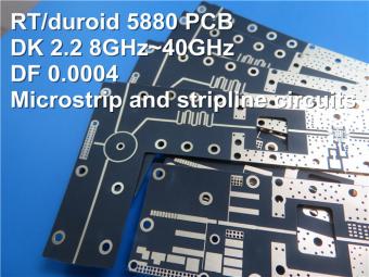
This is a type of double sided RF PCB built on RT/duroid 5880 for the application of Radar Systems.
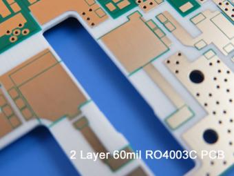
RO4003C PCBs are hydrocarbon ceramic filled laminates, not PTFE which are designed to offer superior high frequency performance.
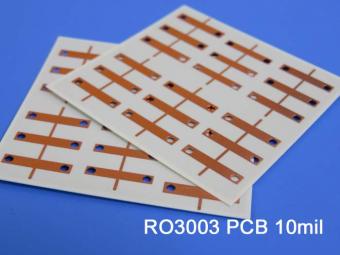
Rogers RO3003 high frequency circuit materials are ceramic-filled PTFE composites intended for use in commercial microwave and RF applications. It was designed to offer exceptional electrical and mechanical stability at competitive prices.
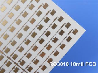
RO3010 laminates are competitively priced products with exceptional mechanical and electrical stability. This stability simplifies the design of broadband components and allows the materials to be used in a wide range of applications over a very broad range of frequencies.
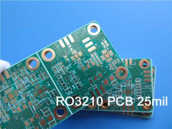
These RO3210 materials are engineered to offer exceptional electrical performance and mechanical stability. RO3210 laminates combine the surface smoothness of a non-woven PTFE laminate.
RT/duroid 6035HTC laminates are an exceptional choice for high power applications.
TC350 is designed to provide enhanced heat-transfer through “Best-In-Class” thermal conductivity, while reducing dielectric loss and insertion loss. Lower losses result in higher Amplifier and Antenna Gains/Efficiencies.
RO3035 materials exhibit a coefficient of thermal expansion(CTE) in the X and Y axis of 17 ppm/℃. This expansion coefficient is matched to that of copper, which allows the material to exhibit excellent dimensional stability.
 6-11C Shidai Jingyuan, Fuyong, Baoan, Shenzhen, Guangdong, China 518103


For inquiries about our products or pricelist, please leave to us and we will be in touch within 24 hours.
© Copyright: 2026 Shenzhen Bicheng Electronics Technology Co., Ltd.. All Rights Reserved.

IPv6 network supported


